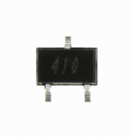
AT-41532-TR1G Avago Technologies US Inc., AT-41532-TR1G Datasheet - Page 2

AT-41532-TR1G
Manufacturer Part Number
AT-41532-TR1G
Description
IC TRANS NPN GP BIPOLAR SOT-323
Manufacturer
Avago Technologies US Inc.
Datasheet
1.AT-41532-BLKG.pdf
(14 pages)
Specifications of AT-41532-TR1G
Transistor Type
NPN
Voltage - Collector Emitter Breakdown (max)
12V
Noise Figure (db Typ @ F)
1dB ~ 1.9dB @ 900MHz ~ 2.4GHz
Gain
9dB ~ 15.5dB
Power - Max
225mW
Dc Current Gain (hfe) (min) @ Ic, Vce
30 @ 5mA, 5V
Current - Collector (ic) (max)
50mA
Mounting Type
Surface Mount
Package / Case
SC-70-3, SOT-323-3
Transistor Polarity
NPN
Collector Emitter Voltage V(br)ceo
12V
Transition Frequency Typ Ft
10GHz
Power Dissipation Pd
225mW
Dc Collector Current
50mA
Dc Current Gain Hfe
150
Lead Free Status / RoHS Status
Lead free / RoHS Compliant
Frequency - Transition
-
Lead Free Status / RoHS Status
Lead free / RoHS Compliant, Lead free / RoHS Compliant
Other names
516-1569-2
Available stocks
Company
Part Number
Manufacturer
Quantity
Price
Company:
Part Number:
AT-41532-TR1G
Manufacturer:
SONY
Quantity:
1 001
Part Number:
AT-41532-TR1G
Manufacturer:
AVAGO/安华高
Quantity:
20 000
AT-41532 Absolute Maximum Ratings
Electrical Specifications, T
Characterization Information, T
2
Symbol
V
V
V
I
P
T
T
Symbol
I
I
Symbol
NF
G
P
G
IP
|S
C
h
CBO
EBO
j
STG
EBO
CBO
CEO
T
1dB
A
1dB
21E
FE
3
|
2
Emitter-Base Voltage
Collector-Base Voltage
Collector-Emitter Voltage
Collector Current
Power Dissipation
Junction Temperature
Storage Temperature
Parameter
Parameters and Test Conditions
Forward Current Transfer Ratio
Collector Cutoff Current
Emitter Cutoff Current
Parameters and Test Conditions
Noise Figure
V
Associated Gain
V
Power at 1 dB Gain Compression (opt tuning)
V
Gain at 1 dB Gain Compression (opt tuning)
V
Output Third Order Intercept Point (opt tuning)
V
Gain in 50 Ω System
V
CE
CE
CE
CE
CE
CE
= 5 V, I
= 5 V, I
= 5 V, I
= 5 V, I
= 5 V, I
= 5 V, I
A
C
C
C
C
C
C
= 25°C
= 5 mA
= 5 mA
= 25 mA
= 25 mA
= 25 mA
= 5 mA
A
[2, 3]
= 25°C
Units
V
V
V
mA
mW
°C
°C
V
I
V
V
C
CE
CB
EB
= 5 mA
= 5 V,
= 1 V
= 3 V
Absolute
Maximum
1.5
20
12
50
225
150
-65 to 150
f = 0.9 GHz
f = 1.8 GHz
f = 2.4 GHz
f = 0.9 GHz
f = 1.8 GHz
f = 2.4 GHz
f = 0.9 GHz
f = 0.9 GHz
f = 2.4 GHz
f = 0.9 GHz
f = 0.9 GHz
Units
–
mA
mA
[1]
Min
30
Units
dB
dB
dBm
dB
dBm
dB
Notes:
1. Operation of this device above any one of
2. T
3. Derate at 2.86 mW/°C for T
these parameters may cause permanent
damage.
> 72°C.
MOUNTING SURFACE
Thermal Resistance
Typ
150
Min
12.5
q
jc
= 350°C/W
= 25°C.
MOUNTING SURFACE
Max
270
0.2
1.0
Typ
1.0
1.4
1.9
15.5
10.5
9.0
14.5
14.5
25
13.25
5.2
[2]:


