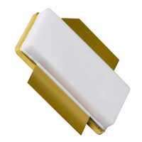
BLF6G10LS-135R,112 NXP Semiconductors, BLF6G10LS-135R,112 Datasheet - Page 2

BLF6G10LS-135R,112
Manufacturer Part Number
BLF6G10LS-135R,112
Description
IC BASESTATION FINAL SOT502B
Manufacturer
NXP Semiconductors
Datasheets
1.BLF6G20LS-140118.pdf
(100 pages)
2.BLF6G20LS-140112.pdf
(110 pages)
3.BLF6G10LS-135R112.pdf
(10 pages)
Specifications of BLF6G10LS-135R,112
Package / Case
SOT502B
Transistor Type
LDMOS
Frequency
871.5MHz
Gain
21dB
Voltage - Rated
65V
Current Rating
32A
Current - Test
950mA
Voltage - Test
28V
Power - Output
26.5W
Configuration
Single
Transistor Polarity
N-Channel
Resistance Drain-source Rds (on)
0.1 Ohms
Drain-source Breakdown Voltage
65 V
Gate-source Breakdown Voltage
13 V
Continuous Drain Current
32 A
Maximum Operating Temperature
+ 225 C
Mounting Style
SMD/SMT
Minimum Operating Temperature
- 65 C
Channel Type
N
Channel Mode
Enhancement
Drain Source Voltage (max)
65V
Output Power (max)
26.5W(Typ)
Power Gain (typ)@vds
21@28VdB
Frequency (min)
869MHz
Frequency (max)
894MHz
Package Type
LDMOST
Pin Count
3
Forward Transconductance (typ)
13S
Drain Source Resistance (max)
100(Typ)@6.15Vmohm
Reverse Capacitance (typ)
2@28VpF
Operating Temp Range
-65C to 225C
Drain Efficiency (typ)
28%
Mounting
Surface Mount
Mode Of Operation
2-Carrier W-CDMA
Number Of Elements
1
Vswr (max)
10
Screening Level
Military
Lead Free Status / RoHS Status
Lead free / RoHS Compliant
Noise Figure
-
Lead Free Status / Rohs Status
Compliant
Other names
934061247112
BLF6G10LS-135R
BLF6G10LS-135R
BLF6G10LS-135R
BLF6G10LS-135R
NXP Semiconductors
2. Pinning information
3. Ordering information
4. Limiting values
5. Thermal characteristics
BLF6G10LS-135R_1
Product data sheet
1.3 Applications
I
Table 2.
[1]
Table 3.
Table 4.
In accordance with the Absolute Maximum Rating System (IEC 60134).
Table 5.
Pin
1
2
3
Type number
BLF6G10LS-135R -
Symbol
V
V
I
T
T
Symbol
R
D
stg
j
DS
GS
th(j-case)
RF power amplifiers for GSM, GSM EDGE, W-CDMA and CDMA base stations and
multi carrier applications in the 800 MHz to 1000 MHz frequency range
Connected to flange.
Parameter
thermal resistance from junction to case
Pinning
Ordering information
Limiting values
Thermal characteristics
Parameter
drain-source voltage
gate-source voltage
drain current
storage temperature
junction temperature
Description
drain
gate
source
Package
Name
Rev. 01 — 17 November 2008
Description
earless flanged LDMOST ceramic package; 2 leads
Conditions
[1]
Simplified outline
Conditions
T
BLF6G10LS-135R
case
= 80 C; P
1
2
3
Power LDMOS transistor
L
= 25 W
Graphic symbol
Min
-
-
-
© NXP B.V. 2008. All rights reserved.
0.5
65
2
Max
65
+13
32
+150
225
sym112
Typ
0.56 K/W
Version
SOT502B
1
3
2 of 10
Unit
Unit
V
V
A
C
C


