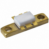
BLF544,112 NXP Semiconductors, BLF544,112 Datasheet - Page 6

BLF544,112
Manufacturer Part Number
BLF544,112
Description
TRANSISTOR RF DMOS SOT171A
Manufacturer
NXP Semiconductors
Datasheet
1.BLF544112.pdf
(16 pages)
Specifications of BLF544,112
Package / Case
SOT-171A
Transistor Type
N-Channel
Frequency
960MHz
Gain
7dB
Voltage - Rated
65V
Current Rating
3.5A
Voltage - Test
28V
Power - Output
20W
Minimum Operating Temperature
- 65 C
Mounting Style
SMD/SMT
Product Type
RF MOSFET Power
Resistance Drain-source Rds (on)
1.25 Ohms
Transistor Polarity
N-Channel
Configuration
Single Quad Source
Drain-source Breakdown Voltage
65 V
Gate-source Breakdown Voltage
+/- 20 V
Continuous Drain Current
3.5 A
Power Dissipation
48 W
Maximum Operating Temperature
+ 200 C
Application
UHF
Channel Type
N
Channel Mode
Enhancement
Drain Source Voltage (max)
65V
Output Power (max)
20W
Power Gain (typ)@vds
14@28VdB
Frequency (max)
960MHz
Package Type
CDFM
Pin Count
6
Forward Transconductance (typ)
0.9S
Drain Source Resistance (max)
1250@10Vmohm
Input Capacitance (typ)@vds
32@28VpF
Output Capacitance (typ)@vds
24@28VpF
Reverse Capacitance (typ)
6.4@28VpF
Operating Temp Range
-65C to 200C
Drain Efficiency (typ)
60%
Mounting
Screw
Mode Of Operation
CW Class-B
Number Of Elements
1
Power Dissipation (max)
48000mW
Vswr (max)
50
Screening Level
Military
Lead Free Status / RoHS Status
Lead free / RoHS Compliant
Noise Figure
-
Current - Test
-
Lead Free Status / Rohs Status
Compliant
Other names
568-2406
933997320112
BLF544
BLF544
933997320112
BLF544
BLF544
Available stocks
Company
Part Number
Manufacturer
Quantity
Price
Company:
Part Number:
BLF544,112
Manufacturer:
Triquint
Quantity:
1 400
Philips Semiconductors
APPLICATION INFORMATION
T
RF performance in a common source class-B circuit.
Ruggedness in class-B operation
The BLF544 is capable of withstanding a full load mismatch corresponding to VSWR = 50 : 1 through all phases under
the following conditions: V
2003 Sep 18
handbook, halfpage
CW, class-B
CW, class-B
CW, class-B
h
MODE OF OPERATION
UHF power MOS transistor
= 25 C; R
V
Fig.8
GS
(pF)
C rs
= 0; f = 1 MHz.
40
30
20
10
0
0
Feedback capacitance as a function of
drain-source voltage; typical values.
th mb-h
= 0.4 K/W unless otherwise specified.
10
DS
= 28 V; f = 500 MHz at rated output power.
(MHz)
500
960
960
20
f
V DS (V)
MDA508
30
V
(V)
28
28
24
DS
6
(mA)
I
40
40
40
DQ
(W)
P
20
20
15
L
typ. 14
typ. 7
typ. 7
(dB)
G
11
p
Product specification
BLF544
typ. 60
typ. 50
typ. 50
(%)
50
D


