BLF544,112 NXP Semiconductors, BLF544,112 Datasheet - Page 4
BLF544,112
Manufacturer Part Number
BLF544,112
Description
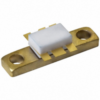
TRANSISTOR RF DMOS SOT171A
Manufacturer
NXP Semiconductors
Datasheet
1.BLF544112.pdf
(16 pages)
Specifications of BLF544,112
Package / Case
SOT-171A
Transistor Type
N-Channel
Frequency
960MHz
Gain
7dB
Voltage - Rated
65V
Current Rating
3.5A
Voltage - Test
28V
Power - Output
20W
Minimum Operating Temperature
- 65 C
Mounting Style
SMD/SMT
Product Type
RF MOSFET Power
Resistance Drain-source Rds (on)
1.25 Ohms
Transistor Polarity
N-Channel
Configuration
Single Quad Source
Drain-source Breakdown Voltage
65 V
Gate-source Breakdown Voltage
+/- 20 V
Continuous Drain Current
3.5 A
Power Dissipation
48 W
Maximum Operating Temperature
+ 200 C
Application
UHF
Channel Type
N
Channel Mode
Enhancement
Drain Source Voltage (max)
65V
Output Power (max)
20W
Power Gain (typ)@vds
14@28VdB
Frequency (max)
960MHz
Package Type
CDFM
Pin Count
6
Forward Transconductance (typ)
0.9S
Drain Source Resistance (max)
1250@10Vmohm
Input Capacitance (typ)@vds
32@28VpF
Output Capacitance (typ)@vds
24@28VpF
Reverse Capacitance (typ)
6.4@28VpF
Operating Temp Range
-65C to 200C
Drain Efficiency (typ)
60%
Mounting
Screw
Mode Of Operation
CW Class-B
Number Of Elements
1
Power Dissipation (max)
48000mW
Vswr (max)
50
Screening Level
Military
Lead Free Status / RoHS Status
Lead free / RoHS Compliant
Noise Figure
-
Current - Test
-
Lead Free Status / Rohs Status
Compliant
Other names
568-2406
933997320112
BLF544
BLF544
933997320112
BLF544
BLF544
Available stocks
Company
Part Number
Manufacturer
Quantity
Price
Company:

Part Number:
BLF544,112
Manufacturer:
Triquint
Quantity:
1 400


Philips Semiconductors
CHARACTERISTICS
T
V
2003 Sep 18
V
I
I
V
g
R
I
C
C
C
j
DSS
GSS
DSX
GS
fs
V
(BR)DSS
GSth
= 25 C unless otherwise specified.
SYMBOL
DSon
is
os
rs
UHF power MOS transistor
GSth
group indicator
GROUP
M
C
D
G
H
N
A
B
E
F
K
J
L
drain-source breakdown voltage
drain-source leakage current
gate-source leakage current
gate-source threshold voltage
gate-source voltage difference of
matched pairs
forward transconductance
drain-source on-state resistance
on-state drain current
input capacitance
output capacitance
feedback capacitance
PARAMETER
MIN.
2.0
2.1
2.2
2.3
2.4
2.5
2.6
2.7
2.8
2.9
3.0
3.1
3.2
LIMITS
(V)
MAX.
2.1
2.2
2.3
2.4
2.5
2.6
2.7
2.8
2.9
3.0
3.1
3.2
3.3
V
V
V
I
I
I
I
V
V
V
V
D
D
D
D
GS
GS
GS
GS
GS
GS
GS
= 40 mA; V
= 40 mA; V
= 1.2 A; V
= 1.2 A; V
4
= 0; I
= 0; V
= 20 V; V
= 15 V; V
= 0; V
= 0; V
= 0; V
D
CONDITIONS
DS
DS
DS
DS
GROUP
= 10 mA
DS
GS
= 28 V
= 28 V; f = 1 MHz
= 28 V; f = 1 MHz
= 28 V; f = 1 MHz
DS
DS
W
DS
O
Q
R
U
P
S
T
V
X
Y
Z
DS
= 10 V
= 10 V
= 10 V
= 10 V
= 10 V
= 0
MIN.
3.3
3.4
3.5
3.6
3.7
3.8
3.9
4.0
4.1
4.2
4.3
4.4
65
1
600
MIN.
LIMITS
900
0.85
4.8
32
24
6.4
(V)
TYP. MAX. UNIT
Product specification
BLF544
1
1
4
100
1.25
MAX.
3.4
3.5
3.6
3.7
3.8
3.9
4.0
4.1
4.2
4.3
4.4
4.5
V
mA
V
mV
mS
A
pF
pF
pF
A
Related parts for BLF544,112
Image
Part Number
Description
Manufacturer
Datasheet
Request
R

Part Number:
Description:
N-channel enhancement mode vertical D-MOS power transistor encapsulated in a 6-lead, SOT171A flange package with a ceramic cap
Manufacturer:
NXP Semiconductors
Datasheet:

Part Number:
Description:
NXP Semiconductors designed the LPC2420/2460 microcontroller around a 16-bit/32-bitARM7TDMI-S CPU core with real-time debug interfaces that include both JTAG andembedded trace
Manufacturer:
NXP Semiconductors
Datasheet:

Part Number:
Description:
NXP Semiconductors designed the LPC2458 microcontroller around a 16-bit/32-bitARM7TDMI-S CPU core with real-time debug interfaces that include both JTAG andembedded trace
Manufacturer:
NXP Semiconductors
Datasheet:
Part Number:
Description:
NXP Semiconductors designed the LPC2468 microcontroller around a 16-bit/32-bitARM7TDMI-S CPU core with real-time debug interfaces that include both JTAG andembedded trace
Manufacturer:
NXP Semiconductors
Datasheet:
Part Number:
Description:
NXP Semiconductors designed the LPC2470 microcontroller, powered by theARM7TDMI-S core, to be a highly integrated microcontroller for a wide range ofapplications that require advanced communications and high quality graphic displays
Manufacturer:
NXP Semiconductors
Datasheet:
Part Number:
Description:
NXP Semiconductors designed the LPC2478 microcontroller, powered by theARM7TDMI-S core, to be a highly integrated microcontroller for a wide range ofapplications that require advanced communications and high quality graphic displays
Manufacturer:
NXP Semiconductors
Datasheet:
Part Number:
Description:
The Philips Semiconductors XA (eXtended Architecture) family of 16-bit single-chip microcontrollers is powerful enough to easily handle the requirements of high performance embedded applications, yet inexpensive enough to compete in the market for hi
Manufacturer:
NXP Semiconductors
Datasheet:
Part Number:
Description:
The XA-S3 device is a member of Philips Semiconductors? XA(eXtended Architecture) family of high performance 16-bitsingle-chip microcontrollers
Manufacturer:
NXP Semiconductors
Datasheet:

Part Number:
Description:
The NXP BlueStreak LH75401/LH75411 family consists of two low-cost 16/32-bit System-on-Chip (SoC) devices
Manufacturer:
NXP Semiconductors
Datasheet:
Part Number:
Description:
The NXP LPC3130/3131 combine an 180 MHz ARM926EJ-S CPU core, high-speed USB2
Manufacturer:
NXP Semiconductors
Datasheet:
Part Number:
Description:
The NXP LPC3141 combine a 270 MHz ARM926EJ-S CPU core, High-speed USB 2
Manufacturer:
NXP Semiconductors
Part Number:
Description:
The NXP LPC3143 combine a 270 MHz ARM926EJ-S CPU core, High-speed USB 2
Manufacturer:
NXP Semiconductors

Part Number:
Description:
The NXP LPC3152 combines an 180 MHz ARM926EJ-S CPU core, High-speed USB 2
Manufacturer:
NXP Semiconductors
Part Number:
Description:
The NXP LPC3154 combines an 180 MHz ARM926EJ-S CPU core, High-speed USB 2
Manufacturer:
NXP Semiconductors