MRFE6S9045NR1 Freescale Semiconductor, MRFE6S9045NR1 Datasheet - Page 3
MRFE6S9045NR1
Manufacturer Part Number
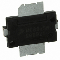
MRFE6S9045NR1
Description
MOSFET RF N-CH 10W TO-270-2
Manufacturer
Freescale Semiconductor
Datasheet
1.MRFE6S9045NR1.pdf
(15 pages)
Specifications of MRFE6S9045NR1
Transistor Type
N-Channel
Frequency
880MHz
Gain
22.1dB
Voltage - Rated
66V
Current Rating
10µA
Current - Test
350mA
Voltage - Test
28V
Power - Output
10W
Package / Case
TO-270-2
Drain Source Voltage Vds
66V
Rf Transistor Case
TO-270
Termination Type
SMD
Output Power Pout
10W
Peak Reflow Compatible (260 C)
Yes
Transistor Polarity
N Channel
Rohs Compliant
Yes
Channel Type
N
Channel Mode
Enhancement
Drain Source Voltage (max)
66V
Output Power (max)
10W
Power Gain (typ)@vds
22.1/20/20dB
Frequency (max)
1GHz
Package Type
TO-270
Pin Count
3
Input Capacitance (typ)@vds
81@28VpF
Output Capacitance (typ)@vds
27@28VpF
Reverse Capacitance (typ)
1.02@28VpF
Operating Temp Range
-65C to 225C
Drain Efficiency (typ)
32%
Mounting
Surface Mount
Mode Of Operation
1-Carrier N-CDMA/CW/GSM EDGE
Number Of Elements
1
Vswr (max)
5
Screening Level
Military
Filter Terminals
SMD
Gate-source Voltage
12V
Leaded Process Compatible
Yes
Operating Frequency Max
880MHz
Lead Free Status / RoHS Status
Contains lead / RoHS Compliant
Noise Figure
-
Lead Free Status / Rohs Status
Compliant
Other names
MRFE6S9045NR1
MRFE6S9045NR1TR
MRFE6S9045NR1TR
Available stocks
Company
Part Number
Manufacturer
Quantity
Price
Company:

Part Number:
MRFE6S9045NR1
Manufacturer:
ELNA
Quantity:
4 000
Part Number:
MRFE6S9045NR1
Manufacturer:
FREESCALE
Quantity:
20 000


RF Device Data
Freescale Semiconductor
Table 5. Electrical Characteristics
Typical GSM EDGE Performances (In Freescale GSM EDGE Test Fixture Optimized for 920 - 960 MHz, 50 ohm system) V
I
Typical CW Performances (In Freescale GSM Test Fixture Optimized for 920 - 960 MHz, 50 ohm system) V
P
Typical Performances (In Freescale Test Fixture, 50 ohm system) V
DQ
out
Power Gain
Drain Efficiency
Error Vector Magnitude
Spectral Regrowth at 400 kHz Offset
Spectral Regrowth at 600 kHz Offset
Power Gain
Drain Efficiency
Input Return Loss
P
Video Bandwidth @ 48 W PEP P
Gain Flatness in 35 MHz Bandwidth @ P
Gain Variation over Temperature
Output Power Variation over Temperature
out
= 350 mA, P
(f = 940 MHz)
(Tone Spacing from 100 kHz to VBW)
ΔIMD3 = IMD3 @ VBW frequency - IMD3 @ 100 kHz <1 dBc (both
sidebands)
( - 30°C to +85°C)
( - 30°C to +85°C)
= 45 W, f = 920 - 960 MHz
@ 1 dB Compression Point
out
= 16 W Avg., f = 920 - 960 MHz, GSM EDGE Signal
Characteristic
out
where IM3 = - 30 dBc
(T
out
C
= 25°C unless otherwise noted)
= 10 W Avg.
DD
= 28 Vdc, I
(continued)
Symbol
ΔP1dB
P1dB
EVM
VBW
SR1
SR2
G
G
IRL
ΔG
η
η
G
ps
ps
D
D
F
DQ
= 350 mA, 865 - 900 MHz Bandwidth
Min
—
—
—
—
—
—
—
—
—
—
—
—
—
0.006
0.011
0.72
Typ
- 62
- 78
- 12
1.5
20
46
20
68
52
10
DD
= 28 Vdc, I
Max
MRFE6S9045NR1
—
—
—
—
—
—
—
—
—
—
—
—
—
DQ
DD
= 350 mA,
= 28 Vdc,
dBm/°C
dB/°C
MHz
Unit
dBc
dBc
dB
dB
dB
dB
W
%
%
%
3
Related parts for MRFE6S9045NR1
Image
Part Number
Description
Manufacturer
Datasheet
Request
R

Part Number:
Description:
Manufacturer:
Freescale Semiconductor, Inc
Datasheet:
Part Number:
Description:
Manufacturer:
Freescale Semiconductor, Inc
Datasheet:
Part Number:
Description:
Manufacturer:
Freescale Semiconductor, Inc
Datasheet:
Part Number:
Description:
Manufacturer:
Freescale Semiconductor, Inc
Datasheet:
Part Number:
Description:
Manufacturer:
Freescale Semiconductor, Inc
Datasheet:
Part Number:
Description:
Manufacturer:
Freescale Semiconductor, Inc
Datasheet:
Part Number:
Description:
Manufacturer:
Freescale Semiconductor, Inc
Datasheet:
Part Number:
Description:
Manufacturer:
Freescale Semiconductor, Inc
Datasheet:
Part Number:
Description:
Manufacturer:
Freescale Semiconductor, Inc
Datasheet:
Part Number:
Description:
Manufacturer:
Freescale Semiconductor, Inc
Datasheet:
Part Number:
Description:
Manufacturer:
Freescale Semiconductor, Inc
Datasheet:
Part Number:
Description:
Manufacturer:
Freescale Semiconductor, Inc
Datasheet:
Part Number:
Description:
Manufacturer:
Freescale Semiconductor, Inc
Datasheet:
Part Number:
Description:
Manufacturer:
Freescale Semiconductor, Inc
Datasheet:
Part Number:
Description:
Manufacturer:
Freescale Semiconductor, Inc
Datasheet: