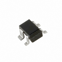
BF908WR,115 NXP Semiconductors, BF908WR,115 Datasheet - Page 4

BF908WR,115
Manufacturer Part Number
BF908WR,115
Description
MOSFET NCH DUAL GATE 12V CMPAK-4
Manufacturer
NXP Semiconductors
Datasheet
1.BF908WR115.pdf
(9 pages)
Specifications of BF908WR,115
Package / Case
CMPAK-4
Transistor Type
N-Channel Dual Gate
Frequency
200MHz
Voltage - Rated
12V
Current Rating
40mA
Noise Figure
0.6dB
Current - Test
15mA
Voltage - Test
8V
Configuration
Single Dual Gate
Continuous Drain Current
0.04 A
Drain-source Breakdown Voltage
12 V
Gate-source Breakdown Voltage
8 V
Maximum Operating Temperature
+ 150 C
Minimum Operating Temperature
- 65 C
Mounting Style
SMD/SMT
Power Dissipation
300 mW
Transistor Polarity
N-Channel
Application
VHF/UHF
Channel Type
N
Channel Mode
Depletion
Drain Source Voltage (max)
12V
Noise Figure (max)
2.5dB
Frequency (max)
1GHz
Package Type
CMPAK
Pin Count
3 +Tab
Input Capacitance (typ)@vds
3.1@8V@Gate 1/1.8@8V@Gate 2pF
Output Capacitance (typ)@vds
1.7@8VpF
Reverse Capacitance (typ)
0.03@8VpF
Operating Temp Range
-65C to 150C
Mounting
Surface Mount
Number Of Elements
1
Power Dissipation (max)
300mW
Screening Level
Military
Lead Free Status / RoHS Status
Lead free / RoHS Compliant
Power - Output
-
Gain
-
Lead Free Status / Rohs Status
Lead free / RoHS Compliant
Other names
568-1969-2
934031470115
BF908WR T/R
934031470115
BF908WR T/R
NXP Semiconductors
THERMAL CHARACTERISTICS
Notes
1. Device mounted on a printed-circuit board.
2. T
STATIC CHARACTERISTICS
T
DYNAMIC CHARACTERISTICS
Common source; T
1995 Apr 25
R
R
V
V
V
V
I
I
I
y
C
C
C
C
F
j
DSS
G1-SS
G2-SS
SYMBOL
SYMBOL
SYMBOL
= 25 C; unless otherwise specified.
(BR)G1-SS
(BR)G2-SS
(P)G1-S
(P)G2-S
N-channel dual-gate MOS-FET
th j-a
th j-s
ig1-s
ig2-s
os
rs
fs
s
is the temperature at the soldering point of the source lead.
thermal resistance from junction to ambient
thermal resistance from junction to soldering point
gate 1-source breakdown voltage V
gate 2-source breakdown voltage V
gate 1-source cut-off voltage
gate 2-source cut-off voltage
drain-source current
gate 1 cut-off current
gate 2 cut-off current
forward transfer admittance
input capacitance at gate 1
input capacitance at gate 2
drain-source capacitance
reverse transfer capacitance f = 1 MHz
noise figure
amb
PARAMETER
= 25 C; V
PARAMETER
PARAMETER
DS
= 8 V; V
G2-S
pulsed; T
f = 1 MHz
f = 1 MHz
f = 1 MHz
f = 200 MHz; G
f = 800 MHz; G
= 4 V; I
V
V
V
V
V
G2-S
G1-S
G2-S
G1-S
G2-S
G2-S
G1-S
j
= 25 C
= V
= V
= 4 V; V
= 4 V; V
= 4 V; V
= V
= V
D
CONDITIONS
= 15 mA; unless otherwise specified.
4
DS
DS
DS
DS
CONDITIONS
S
S
= 2 mS; B
= G
= 0; I
= 0; I
= 0; V
= 0; V
DS
DS
DS
Sopt
= 8 V; I
= 8 V; I
= 8 V; V
G1-S
G2-S
note 1
T
G1-S
G2-S
; B
s
= 87 C; note 2
S
S
= 10 mA
= 10 mA
CONDITIONS
= 5 V
= 5 V
= B
= B
D
D
G1-S
= 20 A
= 20 A
Sopt
Sopt
= 0
8
8
3
36
2.4
1.2
1.2
20
MIN.
MIN.
15
Preliminary specification
43
3.1
1.8
1.7
30
0.6
1.5
TYP.
TYP.
VALUE
350
210
BF908WR
20
20
2
1.5
27
50
50
50
4
2.5
2.2
45
1.2
2.5
MAX.
MAX.
UNIT
K/W
K/W
V
V
V
V
mA
nA
nA
mS
pF
pF
pF
fF
dB
dB
UNIT
UNIT


