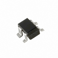
BF908WR,115 NXP Semiconductors, BF908WR,115 Datasheet - Page 3

BF908WR,115
Manufacturer Part Number
BF908WR,115
Description
MOSFET NCH DUAL GATE 12V CMPAK-4
Manufacturer
NXP Semiconductors
Datasheet
1.BF908WR115.pdf
(9 pages)
Specifications of BF908WR,115
Package / Case
CMPAK-4
Transistor Type
N-Channel Dual Gate
Frequency
200MHz
Voltage - Rated
12V
Current Rating
40mA
Noise Figure
0.6dB
Current - Test
15mA
Voltage - Test
8V
Configuration
Single Dual Gate
Continuous Drain Current
0.04 A
Drain-source Breakdown Voltage
12 V
Gate-source Breakdown Voltage
8 V
Maximum Operating Temperature
+ 150 C
Minimum Operating Temperature
- 65 C
Mounting Style
SMD/SMT
Power Dissipation
300 mW
Transistor Polarity
N-Channel
Application
VHF/UHF
Channel Type
N
Channel Mode
Depletion
Drain Source Voltage (max)
12V
Noise Figure (max)
2.5dB
Frequency (max)
1GHz
Package Type
CMPAK
Pin Count
3 +Tab
Input Capacitance (typ)@vds
3.1@8V@Gate 1/1.8@8V@Gate 2pF
Output Capacitance (typ)@vds
1.7@8VpF
Reverse Capacitance (typ)
0.03@8VpF
Operating Temp Range
-65C to 150C
Mounting
Surface Mount
Number Of Elements
1
Power Dissipation (max)
300mW
Screening Level
Military
Lead Free Status / RoHS Status
Lead free / RoHS Compliant
Power - Output
-
Gain
-
Lead Free Status / Rohs Status
Lead free / RoHS Compliant
Other names
568-1969-2
934031470115
BF908WR T/R
934031470115
BF908WR T/R
NXP Semiconductors
LIMITING VALUES
In accordance with the Absolute Maximum Rating System (IEC 134).
Note
1. Device mounted on a printed-circuit board.
1995 Apr 25
handbook, halfpage
V
I
I
I
P
T
T
D
G1
G2
SYMBOL
stg
j
DS
tot
N-channel dual-gate MOS-FET
(mW)
P tot
400
300
200
100
0
0
drain-source voltage
drain current
gate 1 current
gate 2 current
total power dissipation
storage temperature
operating junction temperature
Fig.2 Power derating curve.
50
PARAMETER
100
150
T
amb
MLD154
( C)
o
200
up to T
note 1
amb
CONDITIONS
3
= 45 C; see Fig.2;
65
MIN.
Preliminary specification
12
40
10
10
300
+150
+150
MAX.
BF908WR
V
mA
mA
mA
mW
C
C
UNIT


