BF908WR,115 NXP Semiconductors, BF908WR,115 Datasheet - Page 2
BF908WR,115
Manufacturer Part Number
BF908WR,115
Description
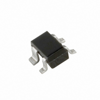
MOSFET NCH DUAL GATE 12V CMPAK-4
Manufacturer
NXP Semiconductors
Datasheet
1.BF908WR115.pdf
(9 pages)
Specifications of BF908WR,115
Package / Case
CMPAK-4
Transistor Type
N-Channel Dual Gate
Frequency
200MHz
Voltage - Rated
12V
Current Rating
40mA
Noise Figure
0.6dB
Current - Test
15mA
Voltage - Test
8V
Configuration
Single Dual Gate
Continuous Drain Current
0.04 A
Drain-source Breakdown Voltage
12 V
Gate-source Breakdown Voltage
8 V
Maximum Operating Temperature
+ 150 C
Minimum Operating Temperature
- 65 C
Mounting Style
SMD/SMT
Power Dissipation
300 mW
Transistor Polarity
N-Channel
Application
VHF/UHF
Channel Type
N
Channel Mode
Depletion
Drain Source Voltage (max)
12V
Noise Figure (max)
2.5dB
Frequency (max)
1GHz
Package Type
CMPAK
Pin Count
3 +Tab
Input Capacitance (typ)@vds
3.1@8V@Gate 1/1.8@8V@Gate 2pF
Output Capacitance (typ)@vds
1.7@8VpF
Reverse Capacitance (typ)
0.03@8VpF
Operating Temp Range
-65C to 150C
Mounting
Surface Mount
Number Of Elements
1
Power Dissipation (max)
300mW
Screening Level
Military
Lead Free Status / RoHS Status
Lead free / RoHS Compliant
Power - Output
-
Gain
-
Lead Free Status / Rohs Status
Lead free / RoHS Compliant
Other names
568-1969-2
934031470115
BF908WR T/R
934031470115
BF908WR T/R


NXP Semiconductors
FEATURES
High forward transfer admittance
Short channel transistor with high forward transfer
Low noise gain controlled amplifier up to 1 GHz.
APPLICATIONS
VHF and UHF applications with 12 V supply voltage,
DESCRIPTION
Depletion type field effect transistor in a plastic
microminiature SOT343R package. The transistor is
protected against excessive input voltage surges by
integrated back-to-back diodes between gates and
source.
QUICK REFERENCE DATA
1995 Apr 25
V
I
P
T
y
C
C
F
The device is supplied in an antistatic package. The
gate-source input must be protected against static
discharge during transport or handling.
D
admittance to input capacitance ratio
such as television tuners and professional
communications equipment.
j
DS
tot
N-channel dual-gate MOS-FET
ig1-s
rs
SYMBOL
fs
drain-source voltage
drain current
total power dissipation
operating junction temperature
forward transfer admittance
input capacitance at gate 1
reverse transfer capacitance
noise figure
CAUTION
PARAMETER
f = 1 MHz
f = 800 MHz
2
PINNING
CONDITIONS
Marking code: MD.
PIN
Fig.1 Simplified outline (SOT343R) and symbol.
1
2
3
4
Top view
3
2
SYMBOL
1
s, b
g
g
d
4
2
1
36
2.4
20
MIN.
source
drain
gate 2
gate 1
MAM198
43
30
3.1
1.5
TYP.
Preliminary specification
DESCRIPTION
g 2
g 1
12
40
300
150
50
4
45
2.5
BF908WR
MAX.
s,b
d
V
mA
mW
C
mS
pF
fF
dB
UNIT
Related parts for BF908WR,115
Image
Part Number
Description
Manufacturer
Datasheet
Request
R

Part Number:
Description:
Depletion type Field-Effect Transistor in a plastic SOT343R package
Manufacturer:
NXP Semiconductors
Datasheet:

Part Number:
Description:
NXP Semiconductors designed the LPC2420/2460 microcontroller around a 16-bit/32-bitARM7TDMI-S CPU core with real-time debug interfaces that include both JTAG andembedded trace
Manufacturer:
NXP Semiconductors
Datasheet:

Part Number:
Description:
NXP Semiconductors designed the LPC2458 microcontroller around a 16-bit/32-bitARM7TDMI-S CPU core with real-time debug interfaces that include both JTAG andembedded trace
Manufacturer:
NXP Semiconductors
Datasheet:
Part Number:
Description:
NXP Semiconductors designed the LPC2468 microcontroller around a 16-bit/32-bitARM7TDMI-S CPU core with real-time debug interfaces that include both JTAG andembedded trace
Manufacturer:
NXP Semiconductors
Datasheet:
Part Number:
Description:
NXP Semiconductors designed the LPC2470 microcontroller, powered by theARM7TDMI-S core, to be a highly integrated microcontroller for a wide range ofapplications that require advanced communications and high quality graphic displays
Manufacturer:
NXP Semiconductors
Datasheet:
Part Number:
Description:
NXP Semiconductors designed the LPC2478 microcontroller, powered by theARM7TDMI-S core, to be a highly integrated microcontroller for a wide range ofapplications that require advanced communications and high quality graphic displays
Manufacturer:
NXP Semiconductors
Datasheet:
Part Number:
Description:
The Philips Semiconductors XA (eXtended Architecture) family of 16-bit single-chip microcontrollers is powerful enough to easily handle the requirements of high performance embedded applications, yet inexpensive enough to compete in the market for hi
Manufacturer:
NXP Semiconductors
Datasheet:
Part Number:
Description:
The XA-S3 device is a member of Philips Semiconductors? XA(eXtended Architecture) family of high performance 16-bitsingle-chip microcontrollers
Manufacturer:
NXP Semiconductors
Datasheet:

Part Number:
Description:
The NXP BlueStreak LH75401/LH75411 family consists of two low-cost 16/32-bit System-on-Chip (SoC) devices
Manufacturer:
NXP Semiconductors
Datasheet:
Part Number:
Description:
The NXP LPC3130/3131 combine an 180 MHz ARM926EJ-S CPU core, high-speed USB2
Manufacturer:
NXP Semiconductors
Datasheet:
Part Number:
Description:
The NXP LPC3141 combine a 270 MHz ARM926EJ-S CPU core, High-speed USB 2
Manufacturer:
NXP Semiconductors
Part Number:
Description:
The NXP LPC3143 combine a 270 MHz ARM926EJ-S CPU core, High-speed USB 2
Manufacturer:
NXP Semiconductors

Part Number:
Description:
The NXP LPC3152 combines an 180 MHz ARM926EJ-S CPU core, High-speed USB 2
Manufacturer:
NXP Semiconductors
Part Number:
Description:
The NXP LPC3154 combines an 180 MHz ARM926EJ-S CPU core, High-speed USB 2
Manufacturer:
NXP Semiconductors