SPU02N60S5 Infineon Technologies, SPU02N60S5 Datasheet - Page 3
SPU02N60S5
Manufacturer Part Number
SPU02N60S5
Description
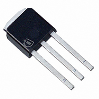
MOSFET N-CH 600V 1.8A TO-251
Manufacturer
Infineon Technologies
Series
CoolMOS™r
Datasheet
1.SPD02N60S5.pdf
(11 pages)
Specifications of SPU02N60S5
Package / Case
IPak, TO-251, DPak (3 straight short leads + tab)
Fet Type
MOSFET N-Channel, Metal Oxide
Fet Feature
Standard
Rds On (max) @ Id, Vgs
3 Ohm @ 1.1A, 10V
Drain To Source Voltage (vdss)
600V
Current - Continuous Drain (id) @ 25° C
1.8A
Vgs(th) (max) @ Id
5.5V @ 80µA
Gate Charge (qg) @ Vgs
9.5nC @ 10V
Input Capacitance (ciss) @ Vds
240pF @ 25V
Power - Max
25W
Mounting Type
Through Hole
Minimum Operating Temperature
- 55 C
Configuration
Single
Transistor Polarity
N-Channel
Resistance Drain-source Rds (on)
3 Ohm @ 10 V
Drain-source Breakdown Voltage
600 V
Gate-source Breakdown Voltage
+/- 20 V
Continuous Drain Current
1.8 A
Power Dissipation
25000 mW
Maximum Operating Temperature
+ 150 C
Mounting Style
SMD/SMT
Fall Time
20 ns
Rise Time
35 ns
Lead Free Status / RoHS Status
Lead free / RoHS Compliant
Lead Free Status / RoHS Status
Lead free / RoHS Compliant, Lead free / RoHS Compliant
Other names
SP000012422
SPU02N60S5
SPU02N60S5IN
SPU02N60S5X
SPU02N60S5XK
SPU02N60S5
SPU02N60S5IN
SPU02N60S5X
SPU02N60S5XK


Gate Charge Characteristics
Gate to source charge
Gate to drain charge
Gate charge total
Gate plateau voltage
1 Repetitve avalanche causes additional power losses that can be calculated as P
2 Device on 40mm*40mm*1.5mm epoxy PCB FR4 with 6cm² (one layer, 70 µm thick) copper area for drain
connection. PCB is vertical without blown air.
Rev. 2.5
Electrical Characteristics , at T
Parameter
Characteristics
Transconductance
Input capacitance
Output capacitance
Reverse transfer capacitance
Turn-on delay time
Rise time
Turn-off delay time
Fall time
Q
Q
Q
V
g
C
C
C
t
t
t
t
Symbol
d(on)
r
d(off)
f
j
(plateau)
fs
gs
gd
g
iss
oss
rss
= 25 °C, unless otherwise specified
V
V
V
V
V
I
V
f=1MHz
V
I
Page 3
D
D
DD
DD
GS
DD
DS
GS
DD
=1.1A
=1.8A, R
=350V, I
=350V, I
=0 to 10V
=350V, I
≥ 2* I
=0V, V
=350V, V
Conditions
D
* R
G
DS
DS(on)max
=50 Ω
D
D
D
GS
=25V,
=1.8A
=1.8A,
=1.8A
=0/10V,
,
min.
-
-
-
-
-
-
-
-
-
-
-
-
AV
=E
AR
Values
typ.
240
2.3
4.5
7.3
*f.
1.4
4.4
77
35
35
35
20
8
SPU02N60S5
SPD02N60S5
2008-04-07
max.
9.5
42
30
-
-
-
-
-
-
-
-
-
nC
V
Unit
S
pF
ns
Related parts for SPU02N60S5
Image
Part Number
Description
Manufacturer
Datasheet
Request
R

Part Number:
Description:
Manufacturer:
Infineon Technologies AG
Datasheet:
Part Number:
Description:
Manufacturer:
Infineon Technologies AG
Datasheet:
Part Number:
Description:
Manufacturer:
Infineon Technologies AG
Datasheet:
Part Number:
Description:
Manufacturer:
Infineon Technologies AG
Datasheet:
Part Number:
Description:
Manufacturer:
Infineon Technologies AG
Datasheet:
Part Number:
Description:
Manufacturer:
Infineon Technologies AG
Datasheet:
Part Number:
Description:
Manufacturer:
Infineon Technologies AG
Datasheet:
Part Number:
Description:
16-bit microcontroller with 2x2 KByte RAM
Manufacturer:
Infineon Technologies AG
Datasheet:
Part Number:
Description:
NPN silicon RF transistor
Manufacturer:
Infineon Technologies AG
Datasheet:
Part Number:
Description:
NPN silicon RF transistor
Manufacturer:
Infineon Technologies AG
Datasheet:
Part Number:
Description:
NPN silicon RF transistor
Manufacturer:
Infineon Technologies AG
Datasheet:
Part Number:
Description:
NPN silicon RF transistor
Manufacturer:
Infineon Technologies AG
Datasheet:
Part Number:
Description:
Si-MMIC-amplifier in SIEGET 25-technologie
Manufacturer:
Infineon Technologies AG
Datasheet:
Part Number:
Description:
IGBT Power Module
Manufacturer:
Infineon Technologies AG
Datasheet:
Part Number:
Description:
IC for switching-mode power supplies
Manufacturer:
Infineon Technologies AG
Datasheet: