BSS87 E6433 Infineon Technologies, BSS87 E6433 Datasheet
BSS87 E6433
Specifications of BSS87 E6433
SP000082233


Related parts for BSS87 E6433


BSS87 E6433 Summary of contents
Page 1
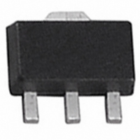
SIPMOS Ò Small-Signal-Transistor Feature · N-Channel · Enhancement mode, Logic Level · dv/dt rated · Pb-free lead plating; RoHS compliant Type Package P-SOT89-4-2 BSS87 Maximum Ratings °C, unless otherwise specified j Parameter Continuous drain current T ...
Page 2
Thermal Characteristics Parameter Characteristics Thermal resistance, junction - case (Pin 2) SMD version, device on PCB: @ min. footprint cooling area Electrical Characteristics Parameter Static Characteristics Drain-source breakdown voltage V =0, I =250µA ...
Page 3
Electrical Characteristics Parameter Dynamic Characteristics Transconductance Input capacitance Output capacitance Reverse transfer capacitance Turn-on delay time Rise time Turn-off delay time Fall time Gate Charge Characteristics Gate to source charge Gate to drain charge Gate charge total Gate ...
Page 4
Power dissipation tot A BSS87 1.1 W 0.9 0.8 0.7 0.6 0.5 0.4 0.3 0.2 0 Safe operating area ...
Page 5
Typ. output characteristic parameter ° 0.52 A 10V 7V 0. 0.4 4.5V 4.1V 0.36 3.5V 2.9V 0.32 2.3V 0.28 0.24 0.2 0.16 0.12 0.08 ...
Page 6
Drain-source on-state resistance DS(on) j parameter : BSS87 98% 6 typ -60 -20 20 ...
Page 7
Typ. gate charge parameter 0.26 A pulsed BSS87 0 max 0 max 6 0 max 4 ...
Page 8
... Infineon Technologies Office. Infineon Technologies components may be used in life-support devices or systems only with the express written approval of Infineon Technologies failure of such components can reasonably be expected to cause the failure of that life-support device or system or to affect the safety or effectiveness of that device or system ...