IRF3711 International Rectifier, IRF3711 Datasheet - Page 2
IRF3711
Manufacturer Part Number
IRF3711
Description
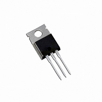
MOSFET N-CH 20V 110A TO-220AB
Manufacturer
International Rectifier
Series
HEXFET®r
Datasheet
1.IRF3711S.pdf
(12 pages)
Specifications of IRF3711
Fet Type
MOSFET N-Channel, Metal Oxide
Fet Feature
Logic Level Gate
Rds On (max) @ Id, Vgs
6 mOhm @ 15A, 10V
Drain To Source Voltage (vdss)
20V
Current - Continuous Drain (id) @ 25° C
110A
Vgs(th) (max) @ Id
3V @ 250µA
Gate Charge (qg) @ Vgs
44nC @ 4.5V
Input Capacitance (ciss) @ Vds
2980pF @ 10V
Power - Max
3.1W
Mounting Type
Through Hole
Package / Case
TO-220-3 (Straight Leads)
Lead Free Status / RoHS Status
Contains lead / RoHS non-compliant
Other names
*IRF3711
Available stocks
Company
Part Number
Manufacturer
Quantity
Price
Company:

Part Number:
IRF3711
Manufacturer:
IR
Quantity:
33 900
Company:
Part Number:
IRF3711
Manufacturer:
GMAMA
Quantity:
25 000
Company:
Part Number:
IRF3711S
Manufacturer:
IR
Quantity:
30 000
Company:
Part Number:
IRF3711SPBF
Manufacturer:
MAXM
Quantity:
5 707
Part Number:
IRF3711STRL
Manufacturer:
IR
Quantity:
20 000
Part Number:
IRF3711STRRPBF
Manufacturer:
IR
Quantity:
20 000
Part Number:
IRF3711TRPBF
Manufacturer:
IR
Quantity:
20 000
Part Number:
IRF3711Z
Manufacturer:
IR
Quantity:
20 000


IRF3711/3711S/3711L
Diode Characteristics
Avalanche Characteristics
Dynamic @ T
Static @ T
t
Symbol
E
I
V
V
∆V
R
V
Symbol
g
Q
Q
Q
Q
Rg
t
t
t
C
C
C
Symbol
I
I
t
Q
t
Q
I
d(on)
AR
I
d(off)
S
SM
rr
rr
DSS
r
f
GSS
fs
AS
2
SD
(BR)DSS
GS(th)
DS(on)
iss
oss
rss
g
gs
gd
oss
rr
rr
(BR)DSS
/∆T
J
Breakdown Voltage Temp. Coefficient
Drain-to-Source Breakdown Voltage
Gate Threshold Voltage
Gate-to-Source Forward Leakage
Gate-to-Source Reverse Leakage
Forward Transconductance
Total Gate Charge
Gate-to-Source Charge
Gate-to-Drain ("Miller") Charge
Output Gate Charge
Gate Resistance
Turn-On Delay Time
Rise Time
Turn-Off Delay Time
Fall Time
Input Capacitance
Output Capacitance
Reverse Transfer Capacitance
Continuous Source Current
(Body Diode)
Pulsed Source Current
(Body Diode)
Reverse Recovery Time
Reverse Recovery Charge
Reverse Recovery Time
Reverse Recovery Charge
Drain-to-Source Leakage Current
Static Drain-to-Source On-Resistance
Diode Forward Voltage
J
= 25°C (unless otherwise specified)
J
Single Pulse Avalanche Energy‚
Avalanche Current
= 25°C (unless otherwise specified)
Parameter
Parameter
Parameter
Parameter
–––
–––
–––
–––
–––
–––
–––
–––
–––
–––
–––
–––
–––
–––
–––
–––
–––
–––
Min. Typ. Max. Units
Min. Typ. Max. Units
1.0
0.3
Min. Typ. Max. Units
20
53
–––
–––
––– 0.88
––– 0.82
–––
–––
–––
–––
0.022
2980 –––
1770 –––
–––
–––
–––
–––
–––
––– -200
–––
–––
220
280
–––
–––
4.7
6.2
7.3
8.9
29
33
12
17
12
50
61
48
65
110
440
–––
100
200
–––
–––
–––
–––
–––
–––
–––
–––
–––
–––
3.0
2.5
1.3
–––
20
44
75
92
72
98
6.0
8.5
†
mΩ
ns
µA
nA
nC
nC
nC
V/°C
pF
ns
ns
V
V
S
Ω
V
Typ.
–––
–––
V
V
V
V
V
V
V
V
V
V
V
V
V
I
R
V
V
V
ƒ = 1.0MHz
MOSFET symbol
showing the
integral reverse
p-n junction diode.
T
T
T
di/dt = 100A/µs ƒ
T
di/dt = 100A/µs ƒ
I
D
D
Reference to 25°C, I
J
J
J
J
GS
GS
GS
DS
DS
DS
GS
GS
DS
DS
GS
GS
DD
G
GS
GS
DS
= 30A
= 15A
= 25°C, I
= 125°C, I
= 25°C, I
= 125°C, I
= 1.8Ω
= V
= 16V, V
= 16V, V
= 16V, I
= 10V
= 10V
= 0V, I
= 10V, I
= 4.5V, I
= 16V
= -16V
= 4.5V
= 0V, V
= 10V
= 4.5V ƒ
= 0V
GS
, I
D
S
F
DS
D
D
D
Conditions
S
F
= 250µA
D
GS
GS
Conditions
= 30A, V
= 16A, V
Conditions
= 250µA
= 15A
= 30A
= 10V
= 30A, V
= 16A, V
= 12A
Max.
460
= 0V, T
= 0V
30
www.irf.com
D
GS
R
ƒ
ƒ
= 1mA
=10V
GS
R
J
=10V
= 125°C
= 0V ƒ
G
= 0V ƒ
Units
mJ
A
D
S
Related parts for IRF3711
Image
Part Number
Description
Manufacturer
Datasheet
Request
R

Part Number:
Description:
SCHOTTKY RECTIFIER
Manufacturer:
International Rectifier Corp.
Datasheet:
Part Number:
Description:
SCHOTTKY RECTIFIER
Manufacturer:
International Rectifier Corp.
Datasheet:
Part Number:
Description:
SCHOTTKY RECTIFIER
Manufacturer:
International Rectifier Corp.
Datasheet:
Part Number:
Description:
SCHOTTKY RECTIFIER
Manufacturer:
International Rectifier Corp.
Datasheet:
Part Number:
Description:
SCHOTTKY RECTIFIER
Manufacturer:
International Rectifier Corp.
Datasheet:
Part Number:
Description:
SCHOTTKY RECTIFIER
Manufacturer:
International Rectifier Corp.
Datasheet:
Part Number:
Description:
SCHOTTKY RECTIFIER
Manufacturer:
International Rectifier Corp.
Datasheet:
Part Number:
Description:
SCHOTTKY RECTIFIER
Manufacturer:
International Rectifier Corp.
Datasheet:
Part Number:
Description:
SCHOTTKY RECTIFIER
Manufacturer:
International Rectifier Corp.
Datasheet:
Part Number:
Description:
SCHOTTKY RECTIFIER
Manufacturer:
International Rectifier Corp.
Datasheet:
Part Number:
Description:
SCHOTTKY RECTIFIER
Manufacturer:
International Rectifier Corp.
Datasheet:
Part Number:
Description:
SCHOTTKY RECTIFIER
Manufacturer:
International Rectifier Corp.
Datasheet:
Part Number:
Description:
SCHOTTKY RECTIFIER
Manufacturer:
International Rectifier Corp.
Datasheet:
Part Number:
Description:
SCHOTTKY RECTIFIER
Manufacturer:
International Rectifier Corp.
Datasheet:
Part Number:
Description:
SCHOTTKY RECTIFIER
Manufacturer:
International Rectifier Corp.
Datasheet: