NTHS4101PT1G ON Semiconductor, NTHS4101PT1G Datasheet
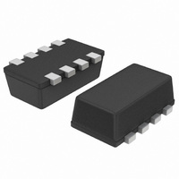
MOSFET P-CH 20V 4.8A CHIPFET

NTHS4101PT1G

Manufacturer Part Number
NTHS4101PT1G
Description
MOSFET P-CH 20V 4.8A CHIPFET
Manufacturer
ON Semiconductor
Datasheet

Specifications of NTHS4101PT1G

Fet Type
MOSFET P-Channel, Metal Oxide
Fet Feature
Logic Level Gate
Rds On (max) @ Id, Vgs
34 mOhm @ 4.8A, 4.5V
Drain To Source Voltage (vdss)
20V
Current - Continuous Drain (id) @ 25° C
4.8A
Vgs(th) (max) @ Id
1.5V @ 250µA
Gate Charge (qg) @ Vgs
35nC @ 4.5V
Input Capacitance (ciss) @ Vds
2100pF @ 16V
Power - Max
1.3W
Mounting Type
Surface Mount
Package / Case
8-ChipFET™
Configuration
Single Hex Drain
Transistor Polarity
P-Channel
Resistance Drain-source Rds (on)
0.034 Ohm @ 4.5 V
Forward Transconductance Gfs (max / Min)
15 S
Drain-source Breakdown Voltage
20 V
Gate-source Breakdown Voltage
+/- 8 V
Continuous Drain Current
4.8 A
Power Dissipation
1300 mW
Mounting Style
SMD/SMT
Lead Free Status / RoHS Status
Lead free / RoHS Compliant
Other names
NTHS4101PT1GOS
NTHS4101PT1GOS
NTHS4101PT1GOSTR

Available stocks

Company
Part Number
Manufacturer
Quantity
Price
Part Number:
NTHS4101PT1G
Manufacturer:
ON
Quantity:
15 000
Part Number:
NTHS4101PT1G
Manufacturer:
ON/安森美
Quantity:
20 000
Part Number:
NTHS4101PT1G
0
Company:
Part Number:
NTHS4101PT1G
Quantity:
3 000
NTHS4101P
Power MOSFET
−20 V, 6.7 A, P−Channel ChipFETt
Features
Applications
Stresses exceeding Maximum Ratings may damage the device. Maximum
Ratings are stress ratings only. Functional operation above the Recommended
Operating Conditions is not implied. Extended exposure to stresses above the
Recommended Operating Conditions may affect device reliability.
1. Surface Mounted on FR4 Board using 1 in sq pad size (Cu area = 1.27 in sq
MAXIMUM RATINGS
© Semiconductor Components Industries, LLC, 2007
February, 2007 − Rev. 3
Drain−to−Source Voltage
Gate−to−Source Voltage − Continuous
Drain Current − Continuous
Total Power Dissipation
Pulsed Drain Current − t
Continuous Source Current
Thermal Resistance (Note 1)
Maximum Lead Temperature for Soldering
making it an Ideal Device for Applications where Board Space is at a
Premium
Environments such as Portable Electronics
Operating Voltage used in many Logic ICs in Portable Electronics
Voltages are not Required
Migration to Lower Levels using the same Basic Topology
Portable Equipment such as MP3 Players, Cell Phones, Digital
Cameras, Personal Digital Assistant and other Portable Applications
Offers an Ultra Low R
Miniature ChipFET Package 40% Smaller Footprint than TSOP−6
Low Profile (<1.1 mm) Allows it to Fit Easily into Extremely Thin
Designed to Provide Low R
Simplifies Circuit Design since Additional Boost Circuits for Gate
Operated at Standard Logic Level Gate Drive, Facilitating Future
Pb−Free Package is Available
Optimized for Battery and Load Management Applications in
Charge Control in Battery Chargers
Buck and Boost Converters
[1 oz] including traces).
Continuous @ T
(5 sec) @ T
Continuous @ 85°C
(5 sec) @ 85°C
Junction−to−Ambient, 5 sec
Junction−to−Ambient, Continuous
Purposes, 1/8″ from case for 10 seconds
A
− 5 seconds
= 25°C
Rating
A
= 25°C
(T
p
J
= 10 ms
DS(on)
= 25°C unless otherwise noted)
DS(on)
Solution in the ChipFET Package
at Gate Voltage as Low as 1.8 V, the
Symbol
V
R
R
V
I
P
T
DSS
DM
I
I
Is
qJA
qJA
GS
D
D
D
L
Value
"8.0
−190
−4.8
−6.7
−4.8
−20
260
1.3
2.5
0.7
1.3
50
95
1
°C/W
Unit
V dc
V dc
°C
W
A
A
A
†For information on tape and reel specifications,
NTHS4101PT1
NTHS4101PT1G
including part orientation and tape sizes, please
refer to our Tape and Reel Packaging Specifications
Brochure, BRD8011/D.
V
D
D
D
(BR)DSS
S
−20 V
CONNECTIONS
Device
8
7
6
5
ORDERING INFORMATION
PIN
1
G
C6 = Specific Device Code
M = Month Code
G = Pb−Free Package
http://onsemi.com
21 mW @ −4.5 V
30 mW @ −2.5 V
42 mW @ −1.8 V
P−Channel MOSFET
1
2
3
4
8
R
(Pb−free)
Package
ChipFET
ChipFET
DS(on)
D
D
D
G
Publication Order Number:
S
TYP
CASE 1206A
D
ChipFET
STYLE 1
1
2
3
4
3000 Tape / Reel
3000 Tape / Reel
MARKING
DIAGRAM
Shipping
NTHS4101P/D
I
D
−6.7 A
MAX
8
7
6
5

Related parts for NTHS4101PT1G

NTHS4101PT1G Summary of contents

Page 1

... DM Is −4.8 A °C qJA R 95 qJA °C T 260 L NTHS4101PT1 NTHS4101PT1G †For information on tape and reel specifications, including part orientation and tape sizes, please refer to our Tape and Reel Packaging Specifications Brochure, BRD8011/D. 1 http://onsemi.com R TYP I MAX DS(on −4 −2.5 V −6 −1.8 V ...

Page 2

ELECTRICAL CHARACTERISTICS Characteristic OFF CHARACTERISTICS Drain−to−Source Breakdown Voltage (Note 2) Temperature Coefficient (Positive) Gate−Body Leakage Current Zero Zero Gate Voltage Drain Current ON CHARACTERISTICS (Note 2) Gate Threshold Voltage Static Drain−to−Source On−Resistance Forward Transconductance Diode Forward Voltage DYNAMIC CHARACTERISTICS Input ...

Page 3

TYPICAL PERFORMANCE CURVES − −2 −1 −1 −1 −1 −V , DRAIN−TO−SOURCE VOLTAGE ...

Page 4

TYPICAL PERFORMANCE CURVES 5000 4500 4000 3500 3000 2500 C rss 2000 1500 1000 C 500 0 −6 −4 − −V − GATE−TO−SOURCE ...

Page 5

... Basic *For additional information on our Pb−Free strategy and soldering details, please download the ON Semiconductor Soldering and Mounting Techniques Reference Manual, SOLDERRM/D. NTHS4101P PACKAGE DIMENSIONS ChipFETt CASE 1206A−03 ISSUE H NOTES: 1. DIMENSIONING AND TOLERANCING PER ANSI Y14.5M, 1982. ...

Page 6

... Opportunity/Affirmative Action Employer. This literature is subject to all applicable copyright laws and is not for resale in any manner. PUBLICATION ORDERING INFORMATION LITERATURE FULFILLMENT: Literature Distribution Center for ON Semiconductor P.O. Box 5163, Denver, Colorado 80217 USA Phone: 303−675−2175 or 800−344−3860 Toll Free USA/Canada Fax: 303− ...

Related keywords