STB45NF06T4 STMicroelectronics, STB45NF06T4 Datasheet - Page 2
STB45NF06T4
Manufacturer Part Number
STB45NF06T4
Description
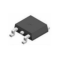
MOSFET N-CH 60V 38A D2PAK
Manufacturer
STMicroelectronics
Series
STripFET™r
Specifications of STB45NF06T4
Fet Type
MOSFET N-Channel, Metal Oxide
Fet Feature
Standard
Rds On (max) @ Id, Vgs
28 mOhm @ 19A, 10V
Drain To Source Voltage (vdss)
60V
Current - Continuous Drain (id) @ 25° C
38A
Vgs(th) (max) @ Id
4V @ 250µA
Gate Charge (qg) @ Vgs
58nC @ 10V
Input Capacitance (ciss) @ Vds
980pF @ 25V
Power - Max
80W
Mounting Type
Surface Mount
Package / Case
DPak, TO-252 (2 leads+tab), SC-63
Configuration
Single
Transistor Polarity
N-Channel
Resistance Drain-source Rds (on)
0.028 Ohm @ 10 V
Drain-source Breakdown Voltage
60 V
Gate-source Breakdown Voltage
+/- 20 V
Continuous Drain Current
38 A
Power Dissipation
80000 mW
Maximum Operating Temperature
+ 175 C
Mounting Style
SMD/SMT
Minimum Operating Temperature
- 65 C
Continuous Drain Current Id
19A
Drain Source Voltage Vds
60V
On Resistance Rds(on)
235mohm
Rds(on) Test Voltage Vgs
10V
Threshold Voltage Vgs Typ
3V
Rohs Compliant
Yes
Lead Free Status / RoHS Status
Lead free / RoHS Compliant
Other names
497-10314-2
STB45NF06T4
STB45NF06T4
Available stocks
Company
Part Number
Manufacturer
Quantity
Price
Company:

Part Number:
STB45NF06T4
Manufacturer:
STMicroelectronics
Quantity:
2 400


STB45NF06
ABSOLUTE MAXIMUM RATINGS
( ) Pulse width limited by safe operating area
(1) I
THERMAL DATA
AVALANCHE CHARACTERISTICS
ELECTRICAL CHARACTERISTICS (T
OFF
ON (1)
2/9
Rthj-case
Rthj-amb
V
dv/dt (1)
Symbol
Symbol
Symbol
Symbol
SD
R
V
I
(BR)DSS
V
DM
P
I
I
V
DS(on)
V
E
GS(th)
T
I
DSS
GSS
DGR
TOT
I
I
AR
T
T
stg
DS
GS
AS
D
D
j
38A, di/dt
l
( )
Avalanche Current, Repetitive or Not-Repetitive
(pulse width limited by T
Single Pulse Avalanche Energy
(starting T
Drain-source
Breakdown Voltage
Zero Gate Voltage
Drain Current (V
Gate-body Leakage
Current (V
Gate Threshold Voltage V
Static Drain-source On
Resistance
Drain-source Voltage (V
Drain-gate Voltage (R
Gate- source Voltage
Drain Current (continuous) at T
Drain Current (continuous) at T
Drain Current (pulsed)
Total Dissipation at T
Derating Factor
Peak Diode Recovery voltage slope
Storage Temperature
Max. Operating Junction Temperature
Thermal Resistance Junction-case Max
Thermal Resistance Junction-ambient Max
Maximum Lead Temperature For Soldering Purpose
300A/µs, V
Parameter
Parameter
j
DS
= 25 °C, I
DD
= 0)
V
GS
(BR)DSS
= 0)
D
C
GS
Parameter
Parameter
= I
= 25°C
GS
, T
j
= 20 k )
max)
AR
I
V
V
V
V
j
D
DS
DS
GS
DS
GS
= 0)
, V
= 250 µA, V
T
CASE
= Max Rating, T
JMAX.
DD
= Max Rating
= ±20V
= V
= 10 V, I
C
C
Test Conditions
Test Conditions
= 25°C
= 100°C
= 50 V)
GS
= 25 °C UNLESS OTHERWISE SPECIFIED)
, I
D
D
GS
= 250µA
= 19 A
= 0
C
= 125°C
Min.
Min.
60
2
–65 to 175
Max Value
Value
0.53
0.022
±20
152
175
1.87
62.5
300
135
60
60
38
26
80
Typ.
Typ.
38
7
3
0.028
Max.
±100
Max.
10
1
4
W/°C
°C/W
°C/W
V/ns
Unit
Unit
Unit
Unit
mJ
µA
µA
nA
°C
°C
°C
W
V
V
V
A
A
A
A
V
V
Related parts for STB45NF06T4
Image
Part Number
Description
Manufacturer
Datasheet
Request
R


Part Number:
Description:
STMicroelectronics [RIPPLE-CARRY BINARY COUNTER/DIVIDERS]
Manufacturer:
STMicroelectronics
Datasheet:
Part Number:
Description:
STMicroelectronics [LIQUID-CRYSTAL DISPLAY DRIVERS]
Manufacturer:
STMicroelectronics
Datasheet:

Part Number:
Description:
BOARD EVAL FOR MEMS SENSORS
Manufacturer:
STMicroelectronics
Datasheet:
Part Number:
Description:
NPN TRANSISTOR POWER MODULE
Manufacturer:
STMicroelectronics
Datasheet:
Part Number:
Description:
TURBOSWITCH ULTRA-FAST HIGH VOLTAGE DIODE
Manufacturer:
STMicroelectronics
Datasheet:
Part Number:
Description:
Manufacturer:
STMicroelectronics
Datasheet:
Part Number:
Description:
DIODE / SCR MODULE
Manufacturer:
STMicroelectronics
Datasheet:
Part Number:
Description:
DIODE / SCR MODULE
Manufacturer:
STMicroelectronics
Datasheet:
Part Number:
Description:
Search -----> STE16N100
Manufacturer:
STMicroelectronics
Datasheet:
Part Number:
Description:
Search ---> STE53NA50
Manufacturer:
STMicroelectronics
Datasheet:
Part Number:
Description:
NPN Transistor Power Module
Manufacturer:
STMicroelectronics
Datasheet: