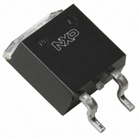
BUK9606-55B,118 NXP Semiconductors, BUK9606-55B,118 Datasheet - Page 9

BUK9606-55B,118
Manufacturer Part Number
BUK9606-55B,118
Description
MOSFET N-CH 55V 75A D2PAK
Manufacturer
NXP Semiconductors
Series
TrenchMOS™r
Datasheet
1.BUK9606-55B118.pdf
(13 pages)
Specifications of BUK9606-55B,118
Package / Case
D²Pak, TO-263 (2 leads + tab)
Mounting Type
Surface Mount
Power - Max
258W
Fet Type
MOSFET N-Channel, Metal Oxide
Gate Charge (qg) @ Vgs
60nC @ 5V
Vgs(th) (max) @ Id
2V @ 1mA
Current - Continuous Drain (id) @ 25° C
75A
Drain To Source Voltage (vdss)
55V
Fet Feature
Logic Level Gate
Rds On (max) @ Id, Vgs
5.4 mOhm @ 25A, 10V
Minimum Operating Temperature
- 55 C
Configuration
Single
Transistor Polarity
N-Channel
Resistance Drain-source Rds (on)
0.0054 Ohm @ 10 V
Drain-source Breakdown Voltage
55 V
Gate-source Breakdown Voltage
15 V
Continuous Drain Current
146 A
Power Dissipation
258000 mW
Maximum Operating Temperature
+ 175 C
Mounting Style
SMD/SMT
Lead Free Status / RoHS Status
Lead free / RoHS Compliant
Lead Free Status / RoHS Status
Lead free / RoHS Compliant, Lead free / RoHS Compliant
Other names
934057312118::BUK9606-55B /T3::BUK9606-55B /T3
NXP Semiconductors
BUK9606-55B_4
Product data sheet
Fig 13. Source current as a function of source-drain
Fig 15. Gate charge waveform definitions
(A)
I
S
100
75
50
25
0
0.0
voltage; typical values
V
V
V
V
GS(pl)
DS
GS(th)
GS
0.2
Q
GS1
I
Q
D
GS
0.4
T
Q
j
= 175 ° C
GS2
Q
G(tot)
0.6
Q
GD
0.8
T
j
003aaa508
= 25 ° C
V
SD
03nj60
(V)
1.0
Rev. 04 — 23 July 2009
Fig 14. Gate-source voltage as a function of gate
Fig 16. Input, output and reverse transfer capacitances
V
(V)
GS
(pF)
8000
6000
4000
2000
C
5
4
3
2
1
0
0
10
charge; typical values
as a function of drain-source voltage; typical
values
0
-1
20
1
V
C
C
C
DD
rss
oss
iss
= 14 V
BUK9606-55B
N-channel TrenchMOS FET
10
40
V
DD
V
© NXP B.V. 2009. All rights reserved.
Q
= 44 V
DS
G
(nC)
(V)
03nj67
03nj61
10
60
2
9 of 13


