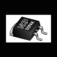
BUK9606-55B NXP Semiconductors, BUK9606-55B Datasheet

BUK9606-55B
Available stocks
Related parts for BUK9606-55B
BUK9606-55B Summary of contents
Page 1
... BUK9606-55B N-channel TrenchMOS FET Rev. 04 — 23 July 2009 1. Product profile 1.1 General description N-channel enhancement mode Field-Effect Transistor (FET plastic package using TrenchMOS technology. This product has been designed and qualified to the appropriate AEC standard for use in automotive critical applications. 1.2 Features and benefits ...
Page 2
... °C; j see Figure 11 and °C; j see Figure 11 and Simplified outline [1] SOT404 (D2PAK) Rev. 04 — 23 July 2009 BUK9606-55B N-channel TrenchMOS FET Min Typ Max - 4 Graphic symbol mbb076 Version SOT404 © NXP B.V. 2009. All rights reserved. ...
Page 3
... °C; unclamped j(init) 03nh85 120 P der (%) 150 200 0 ( ° Fig 2. Normalized total power dissipation as a function of mounting base temperature Rev. 04 — 23 July 2009 BUK9606-55B N-channel TrenchMOS FET Min Max - -15 15 [1] and 3 - 146 [ [ Figure 3 - 587 ...
Page 4
... Safe operating area; continuous and peak drain currents as a function of drain-source voltage BUK9606-55B_4 Product data sheet Limit DSon DS D Capped due to package 1 Rev. 04 — 23 July 2009 BUK9606-55B N-channel TrenchMOS FET 03nh83 = 10 μ 100 μ 100 ms 10 ...
Page 5
... Fig 4. Transient thermal impedance from junction to mounting base as a function of pulse duration BUK9606-55B_4 Product data sheet Conditions see Figure Rev. 04 — 23 July 2009 BUK9606-55B N-channel TrenchMOS FET Min Typ Max - - 0. 03nh84 t p δ ...
Page 6
... °C j from upper edge of drain mounting base to center of die °C j from source lead to source bonding pad °C j Rev. 04 — 23 July 2009 BUK9606-55B N-channel TrenchMOS FET Min Typ Max Unit ...
Page 7
... Drain-source on-state resistance as a function of drain current; typical values 03nj62 100 (A) D Fig 8. Transfer characteristics: drain current as a function of gate-source voltage; typical values Rev. 04 — 23 July 2009 BUK9606-55B N-channel TrenchMOS FET Min Typ Max Unit - 0.85 1 03nj66 3.2 V ...
Page 8
... Fig 10. Sub-threshold drain current as a function of gate-source voltage 03nj64 2 a 1 -60 V (V) GS Fig 12. Normalized drain-source on-state resistance factor as a function of junction temperature Rev. 04 — 23 July 2009 BUK9606-55B N-channel TrenchMOS FET 03ng53 min typ max (V) GS 03ne89 0 60 120 ( ° © ...
Page 9
... Fig 14. Gate-source voltage as a function of gate charge; typical values 8000 C (pF) 6000 4000 2000 GD 003aaa508 0 10 Fig 16. Input, output and reverse transfer capacitances as a function of drain-source voltage; typical values Rev. 04 — 23 July 2009 BUK9606-55B N-channel TrenchMOS FET 03nj61 (nC) G 03nj67 ...
Page 10
... Product data sheet 2 scale max. 1.60 10.30 2.90 15.80 11 2.54 1.20 9.70 2.10 14.80 REFERENCES JEDEC JEITA Rev. 04 — 23 July 2009 BUK9606-55B N-channel TrenchMOS FET mounting base 2.60 2.20 EUROPEAN ISSUE DATE PROJECTION 05-02-11 06-03-16 © NXP B.V. 2009. All rights reserved. SOT404 ...
Page 11
... The format of this data sheet has been redesigned to comply with the new identity guidelines of NXP Semiconductors. • Legal texts have been adapted to the new company name where appropriate. • Type number BUK9606-55B separated from data sheet BUK95_96_9E06_55B_3. BUK95_96_9E06_55B_3 20041130 (9397 750 13519) BUK95_96_9E06_55B-02 ...
Page 12
... Trademarks Notice: All referenced brands, product names, service names and trademarks are the property of their respective owners. TrenchMOS — trademark of NXP B.V. http://www.nxp.com salesaddresses@nxp.com Rev. 04 — 23 July 2009 BUK9606-55B N-channel TrenchMOS FET © NXP B.V. 2009. All rights reserved ...
Page 13
... Please be aware that important notices concerning this document and the product(s) described herein, have been included in section ‘Legal information’. © NXP B.V. 2009. For more information, please visit: http://www.nxp.com For sales office addresses, please send an email to: salesaddresses@nxp.com Document identifier: BUK9606-55B_4 All rights reserved. Date of release: 23 July 2009 ...


