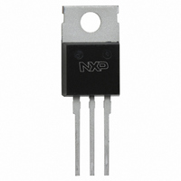
BUK7507-55B,127 NXP Semiconductors, BUK7507-55B,127 Datasheet - Page 5

BUK7507-55B,127
Manufacturer Part Number
BUK7507-55B,127
Description
MOSFET N-CH 55V 75A TO220AB
Manufacturer
NXP Semiconductors
Series
TrenchMOS™r
Datasheet
1.BUK7507-55B127.pdf
(15 pages)
Specifications of BUK7507-55B,127
Package / Case
TO-220AB-3
Mounting Type
Through Hole
Power - Max
203W
Fet Type
MOSFET N-Channel, Metal Oxide
Gate Charge (qg) @ Vgs
53nC @ 10V
Vgs(th) (max) @ Id
4V @ 1mA
Current - Continuous Drain (id) @ 25° C
75A
Drain To Source Voltage (vdss)
55V
Fet Feature
Standard
Rds On (max) @ Id, Vgs
7.1 mOhm @ 25A, 10V
Minimum Operating Temperature
- 55 C
Configuration
Single
Transistor Polarity
N-Channel
Resistance Drain-source Rds (on)
0.0071 Ohm @ 10 V
Drain-source Breakdown Voltage
55 V
Gate-source Breakdown Voltage
+/- 20 V
Continuous Drain Current
119 A
Power Dissipation
203000 mW
Maximum Operating Temperature
+ 175 C
Mounting Style
SMD/SMT
Lead Free Status / RoHS Status
Lead free / RoHS Compliant
Lead Free Status / RoHS Status
Lead free / RoHS Compliant, Lead free / RoHS Compliant
Other names
934057706127::BUK7507-55B::BUK7507-55B
Philips Semiconductors
5. Characteristics
Table 4:
T
9397 750 11235
Product data
Symbol
Static characteristics
V
V
I
I
R
Dynamic characteristics
Q
Q
Q
C
C
C
t
t
t
t
L
L
DSS
GSS
d(on)
r
d(off)
f
j
d
s
(BR)DSS
GS(th)
DSon
iss
oss
rss
g(tot)
gs
gd
= 25 C unless otherwise specified.
Characteristics
Parameter
drain-source breakdown
voltage
gate-source threshold voltage I
drain-source leakage current
gate-source leakage current
drain-source on-state
resistance
total gate charge
gate-source charge
gate-drain (Miller) charge
input capacitance
output capacitance
reverse transfer capacitance
turn-on delay time
rise time
turn-off delay time
fall time
internal drain inductance
internal source inductance
Conditions
I
Figure 9
V
V
V
Figure 7
V
I
V
f = 1 MHz;
V
V
from drain lead 6 mm from
package to center of die
from contact screw on
mounting base to center of
die SOT78
from upper edge of drain
mounting base to center of
die SOT404
from source lead to source
bond pad
D
D
D
DS
GS
GS
GS
GS
DD
GS
T
T
T
T
T
T
T
T
T
= 0.25 mA; V
= 1 mA; V
= 25 A;
j
j
j
j
j
j
j
j
j
= 55 V; V
= 25 C
= 55 C
= 25 C
= 175 C
= 55 C
= 25 C
= 175 C
= 20 V; V
= 10 V; I
= 25 C
= 175 C
= 10 V; V
= 0 V; V
= 30 V; R
= 10 V; R
Rev. 01 — 15 May 2003
and
Figure 14
Figure 12
DS
DS
D
8
GS
DD
L
G
= 25 A;
DS
= V
GS
= 25 V;
= 1.2 ;
= 10
= 0 V
= 44 V;
= 0 V
= 0 V
GS
;
Min
55
50
2
1
-
-
-
-
-
-
-
-
-
-
-
-
-
-
-
-
-
-
-
-
BUK75/7607-55B
TrenchMOS™ standard level FET
© Koninklijke Philips Electronics N.V. 2003. All rights reserved.
Typ
-
-
3
-
-
0.02
-
2
5.8
-
53
12
17
2820
554
200
24
52
77
41
4.5
3.5
2.5
7.5
Max
-
-
4
-
4.4
1
500
100
7.1
14.2
-
-
-
3760
665
274
-
-
-
-
-
-
-
-
Unit
V
V
V
V
V
nA
m
m
nC
nC
nC
pF
pF
pF
ns
ns
ns
ns
nH
nH
nH
nH
5 of 15
A
A


