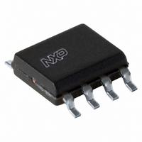
PHK31NQ03LT,518 NXP Semiconductors, PHK31NQ03LT,518 Datasheet - Page 6

PHK31NQ03LT,518
Manufacturer Part Number
PHK31NQ03LT,518
Description
MOSFET N-CH 30V 30.4A 8-SOIC
Manufacturer
NXP Semiconductors
Datasheet
1.PHK31NQ03LT518.pdf
(13 pages)
Specifications of PHK31NQ03LT,518
Package / Case
8-SOIC (3.9mm Width)
Fet Type
MOSFET N-Channel, Metal Oxide
Fet Feature
Logic Level Gate
Rds On (max) @ Id, Vgs
4.4 mOhm @ 25A, 10V
Drain To Source Voltage (vdss)
30V
Current - Continuous Drain (id) @ 25° C
30.4A
Vgs(th) (max) @ Id
2.15V @ 1mA
Gate Charge (qg) @ Vgs
33nC @ 4.5V
Input Capacitance (ciss) @ Vds
4235pF @ 12V
Power - Max
6.9W
Mounting Type
Surface Mount
Minimum Operating Temperature
- 55 C
Mounting Style
SMD/SMT
Configuration
Single Quad Drain Triple Source
Transistor Polarity
N-Channel
Resistance Drain-source Rds (on)
0.0044 Ohm @ 10 V
Drain-source Breakdown Voltage
30 V
Gate-source Breakdown Voltage
+/- 20 V
Continuous Drain Current
30.4 A
Power Dissipation
6900 mW
Maximum Operating Temperature
+ 150 C
Lead Free Status / RoHS Status
Lead free / RoHS Compliant
Lead Free Status / RoHS Status
Lead free / RoHS Compliant, Lead free / RoHS Compliant
Other names
934058879518
PHK31NQ03LT /T3
PHK31NQ03LT /T3
PHK31NQ03LT /T3
PHK31NQ03LT /T3
NXP Semiconductors
Table 6.
PHK31NQ03LT
Product data sheet
Symbol
Source-drain diode
V
t
Q
rr
Fig 5.
Fig 7.
SD
r
(pF)
(A)
C
10
10
I
D
50
40
30
20
10
4
3
0
10
function of drain-source voltage; typical values
function of gate-source voltage; typical values
T
Output characteristics: drain current as a
V
Input and reverse transfer capacitances as a
0
-1
j
GS
Characteristics
= 25 °C
= 0 V; f = 1 MHz
Parameter
source-drain voltage
reverse recovery time
recovered charge
0.2
10 4.5
3.4
…continued
0.4
1
3.2
0.6
V
GS
V
Conditions
I
see
I
V
I
All information provided in this document is subject to legal disclaimers.
S
S
S
GS
V
DS
003aaa692
003aaa698
(V) =
= 25 A; V
= 20 A; dI
= 20 A; dI
DS
(V)
C
C
Figure 15
= 30 V
(V)
iss
rss
2.8
2.6
2.4
3
10
0.8
Rev. 3 — 11 March 2011
GS
S
S
/dt = -100 A/µs; V
/dt = -100 A/µs; V
= 0 V; T
Fig 6.
Fig 8.
j
= 25 °C;
V
GS(th)
(V)
(A)
I
D
1.5
0.5
40
30
20
10
3
2
1
0
0
-60
function of gate-source voltage; typical values
junction temperature
T
Transfer characteristics: drain current as a
Gate-source threshold voltage as a function of
GS
GS
0
j
= 25 °C and 150 °C; V
= 0 V;
= 0 V
N-channel TrenchMOS logic level FET
0
1
T
j
= 150 °C
max
typ
min
PHK31NQ03LT
Min
-
-
-
60
2
DS
25 °C
Typ
0.94
52
30
> I
120
D
3
© NXP B.V. 2011. All rights reserved.
x R
003aaa693
V
003aab272
T
GS
j
(°C)
DSon
Max
1.2
-
-
(V)
180
4
Unit
V
ns
nC
6 of 13


