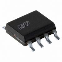
PHK31NQ03LT,518 NXP Semiconductors, PHK31NQ03LT,518 Datasheet

PHK31NQ03LT,518
Specifications of PHK31NQ03LT,518
PHK31NQ03LT /T3
PHK31NQ03LT /T3
Related parts for PHK31NQ03LT,518
PHK31NQ03LT,518 Summary of contents
Page 1
PHK31NQ03LT N-channel TrenchMOS logic level FET Rev. 3 — 11 March 2011 1. Product profile 1.1 General description Logic level N-channel enhancement mode Field-Effect Transistor (FET plastic package using TrenchMOS technology. This product is designed and qualified for ...
Page 2
... NXP Semiconductors 2. Pinning information Table 2. Pinning information Pin Symbol Description 1 S source 2 S source 3 S source 4 G gate 5 D drain 6 D drain 7 D drain 8 D drain 3. Ordering information Table 3. Ordering information Type number Package Name PHK31NQ03LT SO8 PHK31NQ03LT Product data sheet ...
Page 3
... NXP Semiconductors 4. Limiting values Table 4. Limiting values In accordance with the Absolute Maximum Rating System (IEC 60134). Symbol Parameter V drain-source voltage DS V drain-gate voltage DGR V gate-source voltage GS I drain current D I peak drain current DM P total power dissipation tot T storage temperature stg ...
Page 4
... NXP Semiconductors Limit (A) DSon ° single pulse sp DM Fig 3. Safe operating area; continuous and peak drain currents as a function of drain-source voltage 5. Thermal characteristics Table 5. Thermal characteristics Symbol Parameter R thermal resistance from th(j-sp) junction to solder point th(j-sp) (K/W) δ = 0.5 10 0.2 0 ...
Page 5
... NXP Semiconductors 6. Characteristics Table 6. Characteristics Symbol Parameter Static characteristics V drain-source (BR)DSS breakdown voltage V gate-source threshold GS(th) voltage I drain leakage current DSS I gate leakage current GSS R drain-source on-state DSon resistance R gate resistance G Dynamic characteristics Q total gate charge G(tot) Q gate-source charge GS Q pre-threshold ...
Page 6
... NXP Semiconductors Table 6. Characteristics …continued Symbol Parameter Source-drain diode V source-drain voltage SD t reverse recovery time rr Q recovered charge 4 0.2 0 °C j Fig 5. Output characteristics: drain current as a function of drain-source voltage; typical values (pF MHz GS Fig 7. Input and reverse transfer capacitances as a function of gate-source voltage; typical values ...
Page 7
... NXP Semiconductors - ( min - Fig 9. Sub-threshold drain current as a function of gate-source voltage 20 2.6 2.8 R DSon (mΩ °C j Fig 11. Drain-source on-state resistance as a function of drain current; typical values PHK31NQ03LT Product data sheet 003aab271 typ max Fig 10. Normalized drain-source on-state resistance 003aaa694 ...
Page 8
... NXP Semiconductors ° and Fig 13. Gate-source voltage as a function of gate charge; typical values °C and 150 ° Fig 15. Source current as a function of source-drain voltage; typical values PHK31NQ03LT Product data sheet 003aaa695 (pF (nC) G Fig 14. Input, output and reverse transfer capacitances ( 150 °C ...
Page 9
... NXP Semiconductors 7. Package outline SO8: plastic small outline package; 8 leads; body width 3 pin 1 index 1 DIMENSIONS (inch dimensions are derived from the original mm dimensions) A UNIT max. 0.25 1.45 mm 1.75 0.25 0.10 1.25 0.010 0.057 inches 0.069 0.01 0.004 0.049 Notes 1. Plastic or metal protrusions of 0.15 mm (0.006 inch) maximum per side are not included. ...
Page 10
... NXP Semiconductors 8. Revision history Table 7. Revision history Document ID Release date PHK31NQ03LT v.3 20110311 • Modifications: Various changes to content. PHK31NQ03LT v.2 20101220 PHK31NQ03LT Product data sheet Data sheet status Change notice Product data sheet - Product data sheet - All information provided in this document is subject to legal disclaimers. ...
Page 11
... Terms and conditions of commercial sale of NXP Semiconductors. Right to make changes — NXP Semiconductors reserves the right to make changes to information published in this document, including without limitation specifications and product descriptions, at any time and without notice ...
Page 12
... NXP Semiconductors’ specifications such use shall be solely at customer’s own risk, and (c) customer fully indemnifies NXP Semiconductors for any liability, damages or failed product claims resulting from customer design and use of the product for automotive applications beyond NXP Semiconductors’ ...
Page 13
... NXP Semiconductors 11. Contents 1 Product profile . . . . . . . . . . . . . . . . . . . . . . . . . . .1 1.1 General description . . . . . . . . . . . . . . . . . . . . . .1 1.2 Features and benefits . . . . . . . . . . . . . . . . . . . . .1 1.3 Applications . . . . . . . . . . . . . . . . . . . . . . . . . . . .1 1.4 Quick reference data . . . . . . . . . . . . . . . . . . . . .1 2 Pinning information . . . . . . . . . . . . . . . . . . . . . . .2 3 Ordering information . . . . . . . . . . . . . . . . . . . . . .2 4 Limiting values Thermal characteristics . . . . . . . . . . . . . . . . . . .4 6 Characteristics . . . . . . . . . . . . . . . . . . . . . . . . . . .5 7 Package outline . . . . . . . . . . . . . . . . . . . . . . . . . .9 8 Revision history . . . . . . . . . . . . . . . . . . . . . . . . .10 9 Legal information 9.1 Data sheet status ...


