IRF830ALPBF Vishay, IRF830ALPBF Datasheet - Page 7
IRF830ALPBF
Manufacturer Part Number
IRF830ALPBF
Description
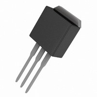
MOSFET N-CH 500V 5A TO262-3
Manufacturer
Vishay
Specifications of IRF830ALPBF
Transistor Polarity
N-Channel
Fet Type
MOSFET N-Channel, Metal Oxide
Fet Feature
Standard
Rds On (max) @ Id, Vgs
1.4 Ohm @ 3A, 10V
Drain To Source Voltage (vdss)
500V
Current - Continuous Drain (id) @ 25° C
5A
Vgs(th) (max) @ Id
4.5V @ 250µA
Gate Charge (qg) @ Vgs
24nC @ 10V
Input Capacitance (ciss) @ Vds
620pF @ 25V
Power - Max
3.1W
Mounting Type
Through Hole
Package / Case
I²Pak, TO-262 (3 straight leads + tab)
Minimum Operating Temperature
- 55 C
Configuration
Single
Resistance Drain-source Rds (on)
1.4 Ohm @ 10 V
Drain-source Breakdown Voltage
500 V
Gate-source Breakdown Voltage
+/- 30 V
Continuous Drain Current
5 A
Power Dissipation
3100 mW
Maximum Operating Temperature
+ 150 C
Mounting Style
Through Hole
Continuous Drain Current Id
5A
Drain Source Voltage Vds
500V
On Resistance Rds(on)
1.4ohm
Rds(on) Test Voltage Vgs
10V
Threshold Voltage Vgs Typ
4.5V
Lead Free Status / RoHS Status
Lead free / RoHS Compliant
Lead Free Status / RoHS Status
Lead free / RoHS Compliant, Lead free / RoHS Compliant
Other names
*IRF830ALPBF


Document Number: 91062
Re-Applied
Voltage
Reverse
Recovery
Current
‚
+
-
R
D.U.T
G
*
Driver Gate Drive
D.U.T. I
D.U.T. V
Inductor Curent
V
GS
Fig 14. For N-Channel HEXFET
= 5V for Logic Level Devices
P.W.
SD
DS
Waveform
Waveform
Peak Diode Recovery dv/dt Test Circuit
Ripple ≤ 5%
Body Diode
Period
Body Diode Forward
+
-
ƒ
• dv/dt controlled by R
• Driver same type as D.U.T.
• I
• D.U.T. - Device Under Test
SD
Diode Recovery
Current
controlled by Duty Factor "D"
Circuit Layout Considerations
dv/dt
Forward Drop
• Low Stray Inductance
• Ground Plane
• Low Leakage Inductance
di/dt
Current Transformer
D =
-
G
Period
®
„
P.W.
Power MOSFET
+
IRF830AS/LPbF
V
V
I
SD
GS
DD
=10V
+
-
V
DD
*
www.vishay.com
7
Related parts for IRF830ALPBF
Image
Part Number
Description
Manufacturer
Datasheet
Request
R

Part Number:
Description:
MOSFET N-CH 500V 4.5A TO-220AB
Manufacturer:
Vishay
Datasheet:

Part Number:
Description:
357-036-542-201 CARDEDGE 36POS DL .156 BLK LOPRO
Manufacturer:
Vishay
Datasheet:
Part Number:
Description:
357-036-542-201 CARDEDGE 36POS DL .156 BLK LOPRO
Manufacturer:
Vishay
Datasheet:
Part Number:
Description:
357-036-542-201 CARDEDGE 36POS DL .156 BLK LOPRO
Manufacturer:
Vishay
Datasheet:
Part Number:
Description:
357-036-542-201 CARDEDGE 36POS DL .156 BLK LOPRO
Manufacturer:
Vishay
Datasheet:
Part Number:
Description:
357-036-542-201 CARDEDGE 36POS DL .156 BLK LOPRO
Manufacturer:
Vishay
Datasheet:
Part Number:
Description:
357-036-542-201 CARDEDGE 36POS DL .156 BLK LOPRO
Manufacturer:
Vishay
Datasheet:
Part Number:
Description:
357-036-542-201 CARDEDGE 36POS DL .156 BLK LOPRO
Manufacturer:
Vishay
Datasheet:
Part Number:
Description:
357-036-542-201 CARDEDGE 36POS DL .156 BLK LOPRO
Manufacturer:
Vishay
Datasheet:
Part Number:
Description:
357-036-542-201 CARDEDGE 36POS DL .156 BLK LOPRO
Manufacturer:
Vishay
Datasheet:
Part Number:
Description:
357-036-542-201 CARDEDGE 36POS DL .156 BLK LOPRO
Manufacturer:
Vishay
Datasheet:
Part Number:
Description:
357-036-542-201 CARDEDGE 36POS DL .156 BLK LOPRO
Manufacturer:
Vishay
Datasheet:
Part Number:
Description:
357-036-542-201 CARDEDGE 36POS DL .156 BLK LOPRO
Manufacturer:
Vishay
Datasheet:
Part Number:
Description:
357-036-542-201 CARDEDGE 36POS DL .156 BLK LOPRO
Manufacturer:
Vishay
Datasheet: