SPB11N60C3 Infineon Technologies, SPB11N60C3 Datasheet
SPB11N60C3
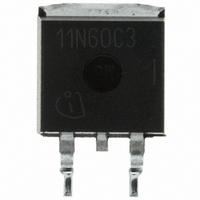
Specifications of SPB11N60C3
SPB11N60C3INTR
SPB11N60C3XT
SPB11N60C3XTINTR
SPB11N60C3XTINTR
Available stocks


Related parts for SPB11N60C3


SPB11N60C3 Summary of contents
Page 1
... Operating and storage temperature 7) Reverse diode dv/dt Rev. 2.6 Ordering Code Q67040-S4396 Symbol puls jmax limited jmax limited jmax tot dv/dt Page 1 SPB11N60C3 @ T 650 V DS jmax R 0.38 DS(on PG-TO263 Marking 11N60C3 Value SPB 340 0.6 11 ±20 ±30 125 T -55...+150 stg 15 2007-12-14 V Ω A Unit ...
Page 2
... GS(th =600V, V =0V, V DSS DS GS =25° =150° =30V, V =0V V GSS GS DS =10V, I =7A V DS(on =25° =150° f=1MHz, open drain R G Page 2 SPB11N60C3 Value Unit 50 V/ns Values Unit min. typ. max K 260 °C Values Unit min. typ. max. 600 - - ...
Page 3
... D r =6.8Ω d(off =480V, I =11A =480V, I =11A 10V =480V, I =11A V D (plateau) DD =400V, V < <T peak BR, DSS j j,max Page 3 SPB11N60C3 Values min. typ. max 1200 - 390 - =0/10V 5 5 while V is rising from 0 to 80% V oss DS while V is rising from 0 to 80% V ...
Page 4
... /dt=100A/µ rrm di /dt =25° Unit Symbol K/W C th1 C th2 C th3 C th4 C th5 C th6 th1 th th1 th2 th,n Page 4 SPB11N60C3 Values min. typ 400 = 1200 Value SPB 0.0001878 0.0007106 0.000988 0.002791 0.007285 0.063 E xternal H eatsink T case Unit max 1.2 V 600 ...
Page 5
... Power dissipation tot C SPP11N60C3 140 W 120 110 100 Safe operating area parameter : =25° 0.001 0. 0 Rev. 2.6 2 Power dissipation FullPAK = tot °C 100 120 160 Safe operating area FullPAK parameter Page 5 SPB11N60C3 ) 100 120 ) DS = 25° 0.001 0. 0 2007-12-14 °C 160 ...
Page 6
... Typ. output characteristic =25° parameter µ 20V A 10V Rev. 2.6 6 Transient thermal impedance FullPAK thJC parameter single pulse - Typ. output characteristic parameter Page 6 SPB11N60C3 ) 0.01 single pulse - =150° µ 20V 2007-12- 5. ...
Page 7
... Rev. 2.6 10 Drain-source on-state resistance R DS(on) parameter : I 2.1 Ω 1.8 6V 5.5V 1.6 1.4 1.2 0.8 0.6 0.4 6.5V 8V 0.2 20V Typ. gate charge = DS(on)max GS parameter 150° Page 7 SPB11N60C3 = SPP11N60C3 1 98% typ 0 -60 - 100 ) Gate = 11 A pulsed D SPP11N60C3 max 0 °C ...
Page 8
... Rev. 2.6 14 Typ. switching time par 2 Typ. drain current slope =125°C di/dt = f(R j =11 A par 3000 A/µs 2000 td(off) 1500 td(on 1000 40 50 Ω Page 8 SPB11N60C3 ), inductive load, T =125° =380V, V =0/+13V td(off td(on inductive load =380V, V =0/+13V, I ...
Page 9
... =11A par mWs 0.025 0.015 0.005 Ω Avalanche SOA =125° =11A par Eon Ω Page 9 SPB11N60C3 ), inductive load, T =125° =380V, V =0/+13V 0.04 *) Eon includes SPD06S60 diode commutation losses 0.03 0.02 Eon* 0.01 Eoff ≤ 150 ° ...
Page 10
... Rev. 2.6 22 Drain-source breakdown voltage V (BR)DSS SPP11N60C3 720 V 680 660 640 620 600 580 560 540 120 °C 160 - Typ. capacitances parameter Page 10 SPB11N60C3 = - 100 °C ) =0V, f=1 MHz GS C iss C oss C rss 100 200 300 400 V 2007-12-14 180 T j 600 V DS ...
Page 11
... Typ. C stored energy oss E =f(V ) oss DS 7.5 µJ 6 5.5 5 4.5 4 3.5 3 2.5 2 1 100 200 300 Definition of diodes switching characteristics Rev. 2.6 400 600 Page 11 SPB11N60C3 2007-12-14 ...
Page 12
... PG-TO263 Rev. 2.6 Page 12 SPB11N60C3 2007-12-14 ...
Page 13
... Life support devices or systems are intended to be implanted in the human body or to support and/or maintain and sustain and/or protect human life. If they fail reasonable to assume that the health of the user or other persons may be endangered. Rev. 2.6 Page 13 SPB11N60C3 2007-12-14 ...