NTA4151PT1G ON Semiconductor, NTA4151PT1G Datasheet
NTA4151PT1G
Specifications of NTA4151PT1G
Available stocks


Related parts for NTA4151PT1G

NTA4151PT1G Summary of contents
Page 1
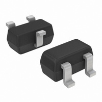
NTA4151P, NTE4151P Small Signal MOSFET −20 V, −760 mA, Single P−Channel, Gate Zener, SC−75, SC−89 Features • Low R for Higher Efficiency and Longer Battery Life DS(on) • Small Outline Package (1.6 x 1.6 mm) • SC−75 Standard Gullwing Package ...
Page 2
... Pulse Test: pulse width ≤ 300 ms, duty cycle ≤ 2%. 3. Switching characteristics are independent of operating junction temperatures. ORDERING INFORMATION Device NTA4151PT1 NTA4151PT1G NTE4151PT1G †For information on tape and reel specifications, including part orientation and tape sizes, please refer to our Tape and Reel Packaging Specifications Brochure, BRD8011/D. NTA4151P, NTE4151P (T = 25° ...
Page 3
... L A1 SOLDERING FOOTPRINT* 1.803 0.071 0.508 0.020 *For additional information on our Pb−Free strategy and soldering details, please download the ON Semiconductor Soldering and Mounting Techniques Reference Manual, SOLDERRM/D. SC−75/SOT−416 CASE 463−01 ISSUE F NOTES: 1. DIMENSIONING AND TOLERANCING PER ANSI Y14.5M, 1982. ...
Page 4
... *For additional information on our Pb−Free strategy and soldering details, please download the ON Semiconductor Soldering and Mounting Techniques Reference Manual, SOLDERRM/D. NTA4151P, NTE4151P SC−89, 3 LEAD CASE 463C−03 ISSUE C NOTES: 1. DIMENSIONING AND TOLERANCING PER ANSI Y14.5M, 1982. 2. CONTROLLING DIMENSION: MILLIMETERS 3 ...