STW26NM50 STMicroelectronics, STW26NM50 Datasheet
STW26NM50
Specifications of STW26NM50
Available stocks


Related parts for STW26NM50


STW26NM50 Summary of contents
Page 1
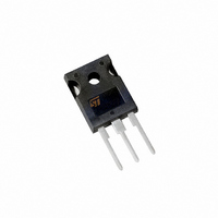
... Table 1. Device summary Order codes STW26NM50 October 2009 N-channel 500 V, 0.10 Ω TO-247 MDmesh™ Power MOSFET R DS(on max < 0.12 Ω Figure 1. Marking W26NM50 Doc ID 8291 Rev 11 STW26NM50 TO-247 Internal schematic diagram Package Packaging TO-247 Tube 1/12 www.st.com 12 ...
Page 2
... Contents Contents 1 Electrical ratings . . . . . . . . . . . . . . . . . . . . . . . . . . . . . . . . . . . . . . . . . . . . 3 2 Electrical characteristics . . . . . . . . . . . . . . . . . . . . . . . . . . . . . . . . . . . . . 4 2.1 Electrical characteristics (curves) 3 Test circuits 4 Package mechanical data . . . . . . . . . . . . . . . . . . . . . . . . . . . . . . . . . . . . . 9 5 Revision history . . . . . . . . . . . . . . . . . . . . . . . . . . . . . . . . . . . . . . . . . . . 11 2/ Doc ID 8291 Rev 11 STW26NM50 . . . . . . . . . . . . . . . . . . . . . . . . . . . . 6 ...
Page 3
... STW26NM50 1 Electrical ratings Table 2. Absolute maximum ratings Symbol V Drain-source voltage ( Gate-source voltage GS I Drain current (continuous Drain current (continuous (1) I Drain current (pulsed Total dissipation at T TOT Derating factor Gate source ESD (HBM-C=100 pF, R=1.5 V ESD(G-S) kΩ) (2) dv/dt Peak diode recovery voltage slope ...
Page 4
... Parameter Test conditions V = MHz 400 (see Figure 15) DS Parameter Test conditions V = 250 4.7 Ω (see Figure 15) Doc ID 8291 Rev 11 STW26NM50 Min. Typ 500 GS =125 ° 250 µ 0.10 D Min. Typ. = 3000 700 - 400 V - 300 = when V oss Min. Typ. Max. Unit = 13 A, ...
Page 5
... STW26NM50 Table 8. Source drain diode Symbol I Source-drain current SD (1) I Source-drain current (pulsed) SDM (2) V Forward on voltage SD t Reverse recovery time rr Q Reverse recovery charge rr I Reverse recovery current RRM t Reverse recovery time rr Q Reverse recovery charge rr I Reverse recovery current RRM 1. Pulse width limited by safe operating area 2. Pulsed: pulse duration = 300 µ ...
Page 6
... Electrical characteristics 2.1 Electrical characteristics (curves) Figure 2. Safe operating area Figure 4. Output characteristics Figure 6. Transconductance 6/12 Figure 3. Thermal impedance Figure 5. Transfer characteristics Figure 7. Static drain-source on resistance Doc ID 8291 Rev 11 STW26NM50 ...
Page 7
... STW26NM50 Figure 8. Gate charge vs gate-source voltage Figure 9. Figure 10. Normalized gate threshold voltage vs temperature Figure 12. Source-drain diode forward characteristics Capacitance variations Figure 11. Normalized on resistance vs temperature Figure 13. Normalized B BV DSS (norm) 1. 1.04 1.00 0.96 0.92 -75 -50 -25 Doc ID 8291 Rev 11 Electrical characteristics vs temperature VDSS ...
Page 8
... AM01468v1 Figure 17. Unclamped inductive load test 3.3 1000 µF µ AM01470v1 Figure 19. Switching time waveform V (BR)DSS 10% 0 AM01472v1 Doc ID 8291 Rev 11 STW26NM50 12V 47kΩ 100nF I =CONST G 100Ω GMAX 2200 µF 2.7kΩ 47kΩ 1kΩ circuit 2200 3.3 µ ...
Page 9
... STW26NM50 4 Package mechanical data In order to meet environmental requirements, ST offers these devices in different grades of ® ECOPACK packages, depending on their level of environmental compliance. ECOPACK specifications, grade definitions and product status are available at: www.st.com. ECOPACK trademark. Doc ID 8291 Rev 11 Package mechanical data ® 9/12 ...
Page 10
... L1 L2 øP øR S 10/12 TO-247 mechanical data mm. Min. Typ. 4.85 2.20 1.0 2.0 3.0 0.40 19.85 15.45 5.45 14.20 3.70 18.50 3.55 4.50 5.50 Doc ID 8291 Rev 11 STW26NM50 Max. 5.15 2.60 1.40 2.40 3.40 0.80 20.15 15.75 14.80 4.30 3.65 5.50 ...
Page 11
... STW26NM50 5 Revision history Table 10. Document revision history Date 24-Jun-2004 07-Feb-2005 02-Oct-2009 Revision 9 New stylesheet value changed D 11 Modified: test condition of V Doc ID 8291 Rev 11 Revision history Changes Table 5 in (BR)DSS 11/12 ...
Page 12
... Australia - Belgium - Brazil - Canada - China - Czech Republic - Finland - France - Germany - Hong Kong - India - Israel - Italy - Japan - Malaysia - Malta - Morocco - Philippines - Singapore - Spain - Sweden - Switzerland - United Kingdom - United States of America 12/12 Please Read Carefully: © 2009 STMicroelectronics - All rights reserved STMicroelectronics group of companies www.st.com Doc ID 8291 Rev 11 STW26NM50 ...