STV200N55F3 STMicroelectronics, STV200N55F3 Datasheet
STV200N55F3
Specifications of STV200N55F3


Related parts for STV200N55F3


STV200N55F3 Summary of contents
Page 1
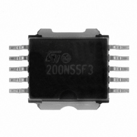
... STV200N55F3 March 2009 N-channel 55 V, 1.8 mΩ, 200 A, PowerSO-10 STripFET™ Power MOSFET R DS(on) ( max < 2.5 mΩ 200 A Figure 1. Marking 200N55F3 PowerSO-10 Rev 3 STV200N55F3 10 1 PowerSO-10 Internal schematic diagram and connection diagram (top view) Package Packaging Tape and reel 1/12 www.st.com 12 ...
Page 2
... Contents Contents 1 Electrical ratings . . . . . . . . . . . . . . . . . . . . . . . . . . . . . . . . . . . . . . . . . . . . 3 2 Electrical characteristics . . . . . . . . . . . . . . . . . . . . . . . . . . . . . . . . . . . . . 4 2.1 Electrical characteristics (curves) 3 Test circuits 4 Package mechanical data . . . . . . . . . . . . . . . . . . . . . . . . . . . . . . . . . . . . . 9 5 Revision history . . . . . . . . . . . . . . . . . . . . . . . . . . . . . . . . . . . . . . . . . . . 11 2/ STV200N55F3 ...
Page 3
... STV200N55F3 1 Electrical ratings Table 2. Absolute maximum ratings Symbol V Drain-source voltage ( Gate-source voltage GS (1) I Drain current (continuous Drain current (continuous (2) I Drain current (pulsed) DM (3) P Total dissipation at T TOT Derating factor (4) E Single pulse avalanche energy AS T Storage temperature stg T Operating junction temperature j 1 ...
Page 4
... Gate-drain charge gd 4/12 Test conditions I = 250 µ Max rating Max rating ± 250 µ Test conditions MHz 120 Figure 14 STV200N55F3 Min. Typ. Max 125 ° ±100 2 4 1.8 2.5 Min. Typ. Max. 6800 =0 1450 GS 15 100 30 26 Unit V µA µ mΩ Unit ...
Page 5
... STV200N55F3 Table 6. Switching times Symbol t Turn-on delay time d(on) t Rise time r t Turn-off delay time d(off) t Fall time f Table 7. Source drain diode Symbol I Source-drain current SD (1) I Source-drain current (pulsed) SD (2) V Forward on voltage SD t Reverse recovery time rr Q Reverse recovery charge rr I Reverse recovery current RRM 1 ...
Page 6
... DS 10 Figure 5. AM03161v1 I D (A) 400 6V 350 300 250 200 150 100 ( temperature Figure 7. R DS(on) (Ω) 2.5 2.0 1.5 1.0 0.5 STV200N55F3 Thermal impedance 280tok δ=0.5 0.2 0.1 0.05 0.02 Zth=k Rthj-c δ=tp/τ 0.01 Single pulse tp τ Transfer characteristics V = ...
Page 7
... STV200N55F3 Figure 8. Gate charge vs gate-source voltage Figure 9. Figure 10. Normalized gate threshold voltage vs temperature Figure 12. Source-drain diode forward characteristics Electrical characteristics Capacitance variations Figure 11. Normalized on resistance vs temperature 7/12 ...
Page 8
... Test circuits Figure 13. Switching times test circuit for resistive load Figure 15. Test circuit for inductive load switching and diode recovery times Figure 17. Unclamped inductive waveform 8/12 Figure 14. Gate charge test circuit Figure 16. Unclamped inductive load test circuit Figure 18. Switching time waveform STV200N55F3 ...
Page 9
... STV200N55F3 4 Package mechanical data In order to meet environmental requirements, ST offers these devices in different grades of ® ECOPACK packages, depending on their level of environmental compliance. ECOPACK specifications, grade definitions and product status are available at: www.st.com. ECOPACK trademark. Package mechanical data ® 9/12 ...
Page 10
... Package mechanical data Dim < 10/12 PowerSO-10 mechanical data mm Min Typ 0.00 3.40 1.25 0.40 0.35 9.40 7.40 13.80 9.30 7.20 5.90 1.27 0. STV200N55F3 Max 3.70 0.10 3.60 1.35 0.53 0.55 9.60 7.60 14.40 9.50 7.60 6.10 1. 0068039_E ...
Page 11
... STV200N55F3 5 Revision history Table 8. Document revision history Date 05-Mar-2008 10-Nov-2008 02-Mar-2009 Revision 1 First release. 2 Document status promoted from preliminary to datasheet. Figure 2 3 has been updated. Revision history Changes 11/12 ...
Page 12
... Australia - Belgium - Brazil - Canada - China - Czech Republic - Finland - France - Germany - Hong Kong - India - Israel - Italy - Japan - Malaysia - Malta - Morocco - Singapore - Spain - Sweden - Switzerland - United Kingdom - United States of America 12/12 Please Read Carefully: © 2009 STMicroelectronics - All rights reserved STMicroelectronics group of companies www.st.com STV200N55F3 ...