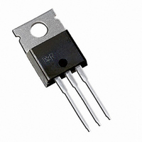
IRLIB9343PBF International Rectifier, IRLIB9343PBF Datasheet - Page 3

IRLIB9343PBF
Manufacturer Part Number
IRLIB9343PBF
Description
MOSFET P-CH 55V 14A TO220FP
Manufacturer
International Rectifier
Series
HEXFET®r
Type
Power MOSFETr
Datasheet
1.IRLIB9343PBF.pdf
(8 pages)
Specifications of IRLIB9343PBF
Fet Type
MOSFET P-Channel, Metal Oxide
Fet Feature
Standard
Rds On (max) @ Id, Vgs
105 mOhm @ 3.4A, 10V
Drain To Source Voltage (vdss)
55V
Current - Continuous Drain (id) @ 25° C
14A
Vgs(th) (max) @ Id
1V @ 250µA
Gate Charge (qg) @ Vgs
47nC @ 10V
Input Capacitance (ciss) @ Vds
660pF @ 50V
Power - Max
33W
Mounting Type
Through Hole
Package / Case
TO-220-3 Full Pack (Straight Leads)
Configuration
Single
Transistor Polarity
P-Channel
Resistance Drain-source Rds (on)
170 mOhms
Drain-source Breakdown Voltage
- 55 V
Gate-source Breakdown Voltage
20 V
Continuous Drain Current
- 14 A
Power Dissipation
33 W
Maximum Operating Temperature
+ 175 C
Mounting Style
Through Hole
Fall Time
9.5 ns
Gate Charge Qg
31 nC
Minimum Operating Temperature
- 40 C
Rise Time
24 ns
Number Of Elements
1
Polarity
P
Channel Mode
Enhancement
Drain-source On-res
0.105Ohm
Drain-source On-volt
55V
Gate-source Voltage (max)
±20V
Operating Temp Range
-40C to 175C
Operating Temperature Classification
Automotive
Mounting
Through Hole
Pin Count
3 +Tab
Package Type
TO-220AB Full-Pak
Lead Free Status / RoHS Status
Lead free / RoHS Compliant
Other names
*IRLIB9343PBF
Fig 5. Typical Capacitance vs.Drain-to-Source Voltage
www.irf.com
100.0
10000
10.0
1000
Fig 3. Typical Transfer Characteristics
100
1.0
0.1
100
0.1
10
10
1
Fig 1. Typical Output Characteristics
0.0
0.1
1
-V GS , Gate-to-Source Voltage (V)
-V DS , Drain-to-Source Voltage (V)
-V DS , Drain-to-Source Voltage (V)
T J = 25°C
V GS = 0V,
C iss = C gs + C gd , C ds SHORTED
C rss = C gd
C oss = C ds + C gd
5.0
1
-2.5V
V DS = -25V
≤ 60µs PULSE WIDTH
≤ 60µs PULSE WIDTH
Tj = 25°C
f = 1 MHZ
10
Coss
Ciss
Crss
10.0
10
TOP
BOTTOM
T J = 175°C
VGS
-15V
-12V
-10V
-8.0V
-5.5V
-4.5V
-3.0V
-2.5V
15.0
100
100
Fig 6. Typical Gate Charge vs.Gate-to-Source Voltage
Fig 4. Normalized On-Resistance vs. Temperature
2.0
1.5
1.0
0.5
100
Fig 2. Typical Output Characteristics
0.1
20
16
12
10
-60 -40 -20 0
1
8
4
0
0.1
0
I D = -14A
V GS = -10V
I D = -14A
-V DS , Drain-to-Source Voltage (V)
T J , Junction Temperature (°C)
10
Q G Total Gate Charge (nC)
20 40 60 80 100 120 140 160 180
1
V DS = -44V
VDS= -28V
VDS= -11V
20
-2.5V
≤ 60µs PULSE WIDTH
Tj = 175°C
FOR TEST CIRCUIT
SEE FIGURE 19
30
10
TOP
BOTTOM
40
VGS
-15V
-12V
-10V
-8.0V
-5.5V
-4.5V
-3.0V
-2.5V
3
100
50


