IRFR3504ZTRPBF International Rectifier, IRFR3504ZTRPBF Datasheet - Page 2
IRFR3504ZTRPBF
Manufacturer Part Number
IRFR3504ZTRPBF
Description
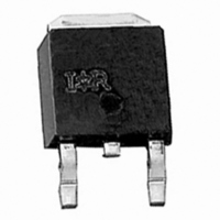
MOSFET N-CH 40V 42A DPAK
Manufacturer
International Rectifier
Series
HEXFET®r
Datasheet
1.IRFR3504ZTRPBF.pdf
(11 pages)
Specifications of IRFR3504ZTRPBF
Fet Type
MOSFET N-Channel, Metal Oxide
Fet Feature
Standard
Rds On (max) @ Id, Vgs
9 mOhm @ 42A, 10V
Drain To Source Voltage (vdss)
40V
Current - Continuous Drain (id) @ 25° C
42A
Vgs(th) (max) @ Id
4V @ 250µA
Gate Charge (qg) @ Vgs
45nC @ 10V
Input Capacitance (ciss) @ Vds
1510pF @ 25V
Power - Max
90W
Mounting Type
Surface Mount
Package / Case
DPak, TO-252 (2 leads+tab), SC-63
Transistor Polarity
N Channel
Continuous Drain Current Id
77A
Drain Source Voltage Vds
40V
On Resistance Rds(on)
9mohm
Rds(on) Test Voltage Vgs
10V
Peak Reflow Compatible (260 C)
Yes
Rohs Compliant
Yes
Lead Free Status / RoHS Status
Lead free / RoHS Compliant
Other names
IRFR3504ZPBFTR
IRFR3504ZTRPBF
IRFR3504ZTRPBFTR
IRFR3504ZTRPBF
IRFR3504ZTRPBFTR
Available stocks
Company
Part Number
Manufacturer
Quantity
Price
Company:

Part Number:
IRFR3504ZTRPBF
Manufacturer:
International Rectifier
Quantity:
64 748


Electrical Characteristics @ T
V
R
V
gfs
I
I
Q
Q
Q
t
t
t
t
L
L
C
C
C
C
C
C
Source-Drain Ratings and Characteristics
I
I
V
t
Q
t
DSS
GSS
d(on)
r
d(off)
f
S
SM
rr
on
D
S
2
V
(BR)DSS
DS(on)
GS(th)
iss
oss
rss
oss
oss
oss
SD
g
gs
gd
rr
(BR)DSS
eff.
/ T
J
Drain-to-Source Breakdown Voltage
Breakdown Voltage Temp. Coefficient
Static Drain-to-Source On-Resistance
Gate Threshold Voltage
Forward Transconductance
Drain-to-Source Leakage Current
Gate-to-Source Forward Leakage
Gate-to-Source Reverse Leakage
Total Gate Charge
Gate-to-Source Charge
Gate-to-Drain ("Miller") Charge
Turn-On Delay Time
Rise Time
Turn-Off Delay Time
Fall Time
Internal Drain Inductance
Internal Source Inductance
Input Capacitance
Output Capacitance
Reverse Transfer Capacitance
Output Capacitance
Output Capacitance
Effective Output Capacitance
Continuous Source Current
(Body Diode)
Pulsed Source Current
(Body Diode)
Diode Forward Voltage
Reverse Recovery Time
Reverse Recovery Charge
Forward Turn-On Time
Parameter
Parameter
™
J
= 25°C (unless otherwise specified)
Intrinsic turn-on time is negligible (turn-on is dominated by LS+LD)
Min. Typ. Max. Units
Min. Typ. Max. Units
–––
–––
–––
–––
–––
–––
–––
–––
–––
–––
–––
–––
–––
–––
–––
–––
–––
–––
–––
–––
–––
–––
–––
–––
–––
–––
2.0
40
32
0.032
1510
1100
8.23
–––
–––
–––
–––
–––
–––
–––
340
190
340
460
–––
–––
–––
9.6
4.5
7.5
9.2
30
12
15
74
30
38
18
-200
–––
–––
–––
250
200
–––
–––
–––
–––
–––
–––
–––
–––
–––
–––
–––
–––
–––
–––
310
9.0
4.0
1.3
20
45
42
27
14
V/°C
m
nC
nH
nC
µA
nA
ns
pF
ns
V
V
S
A
V
V
Reference to 25°C, I
V
V
V
V
V
V
V
I
V
V
V
I
R
V
Between lead,
6mm (0.25in.)
from package
and center of die contact
V
V
ƒ = 1.0MHz
V
V
V
MOSFET symbol
showing the
integral reverse
p-n junction diode.
T
T
di/dt = 100A/µs
D
D
J
J
GS
GS
DS
DS
DS
DS
GS
GS
DS
GS
DD
GS
GS
DS
GS
GS
GS
G
= 42A
= 42A
= 25°C, I
= 25°C, I
= 15
= 0V, I
= 10V, I
= V
= 10V, I
= 40V, V
= 40V, V
= 20V
= -20V
= 32V
= 10V
= 20V
= 10V
= 0V
= 25V
= 0V, V
= 0V, V
= 0V, V
GS
, I
e
e
D
Conditions
Conditions
D
S
F
DS
D
D
DS
DS
= 250µA
GS
GS
= 250µA
= 42A, V
= 42A, V
= 42A
= 42A
= 0V to 32V
= 1.0V, ƒ = 1.0MHz
= 32V, ƒ = 1.0MHz
e
= 0V
= 0V, T
www.irf.com
D
e
= 1mA
GS
DD
J
= 125°C
= 20V
= 0V
G
f
e
S
D
Related parts for IRFR3504ZTRPBF
Image
Part Number
Description
Manufacturer
Datasheet
Request
R

Part Number:
Description:
MOSFET N-CH 40V 42A DPAK
Manufacturer:
International Rectifier
Datasheet:

Part Number:
Description:
40v Single N-channel Hexfet Power Mosfet In A I-pak Package
Manufacturer:
International Rectifier Corp.
Datasheet:
Part Number:
Description:
SCHOTTKY RECTIFIER
Manufacturer:
International Rectifier Corp.
Datasheet:
Part Number:
Description:
SCHOTTKY RECTIFIER
Manufacturer:
International Rectifier Corp.
Datasheet:
Part Number:
Description:
SCHOTTKY RECTIFIER
Manufacturer:
International Rectifier Corp.
Datasheet:
Part Number:
Description:
SCHOTTKY RECTIFIER
Manufacturer:
International Rectifier Corp.
Datasheet:
Part Number:
Description:
SCHOTTKY RECTIFIER
Manufacturer:
International Rectifier Corp.
Datasheet:
Part Number:
Description:
SCHOTTKY RECTIFIER
Manufacturer:
International Rectifier Corp.
Datasheet:
Part Number:
Description:
SCHOTTKY RECTIFIER
Manufacturer:
International Rectifier Corp.
Datasheet:
Part Number:
Description:
SCHOTTKY RECTIFIER
Manufacturer:
International Rectifier Corp.
Datasheet:
Part Number:
Description:
SCHOTTKY RECTIFIER
Manufacturer:
International Rectifier Corp.
Datasheet:
Part Number:
Description:
SCHOTTKY RECTIFIER
Manufacturer:
International Rectifier Corp.
Datasheet:
Part Number:
Description:
SCHOTTKY RECTIFIER
Manufacturer:
International Rectifier Corp.
Datasheet:
Part Number:
Description:
SCHOTTKY RECTIFIER
Manufacturer:
International Rectifier Corp.
Datasheet:
Part Number:
Description:
SCHOTTKY RECTIFIER
Manufacturer:
International Rectifier Corp.
Datasheet: