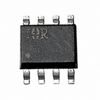
IRF7353D2TRPBF International Rectifier, IRF7353D2TRPBF Datasheet - Page 2

IRF7353D2TRPBF
Manufacturer Part Number
IRF7353D2TRPBF
Description
MOSFET N-CH 30V 6.5A 8-SOIC
Manufacturer
International Rectifier
Series
FETKY™r
Datasheet
1.IRF7353D2TRPBF.pdf
(8 pages)
Specifications of IRF7353D2TRPBF
Fet Type
MOSFET N-Channel, Metal Oxide
Fet Feature
Diode (Isolated)
Rds On (max) @ Id, Vgs
29 mOhm @ 5.8A, 10V
Drain To Source Voltage (vdss)
30V
Current - Continuous Drain (id) @ 25° C
6.5A
Vgs(th) (max) @ Id
1V @ 250µA
Gate Charge (qg) @ Vgs
33nC @ 10V
Input Capacitance (ciss) @ Vds
650pF @ 25V
Power - Max
2W
Mounting Type
Surface Mount
Package / Case
8-SOIC (3.9mm Width)
Transistor Polarity
N-Channel
Resistance Drain-source Rds (on)
46 mOhms
Drain-source Breakdown Voltage
30 V
Gate-source Breakdown Voltage
20 V
Continuous Drain Current
6.5 A
Power Dissipation
2 W
Mounting Style
SMD/SMT
Gate Charge Qg
22 nC
Lead Free Status / RoHS Status
Lead free / RoHS Compliant
Other names
IRF7353D2PBFTR
IRF7353D2TRPBF
IRF7353D2TRPBFTR
IRF7353D2TRPBF
IRF7353D2TRPBFTR
IRF7353D2PbF
MOSFET Electrical Characteristics @ T
MOSFET Source-Drain Ratings and Characteristics
Schottky Diode Electrical Specifications
Schottky Diode Maximum Ratings
( HEXFET is the reg. TM for International Rectifier Power MOSFET's )
I
I
V
I
C
dv/dt
Parameter
V
R
V
g
I
I
Q
Q
Q
t
t
t
t
C
C
C
Parameter
I
I
V
t
Q
SM
F (av)
rm
DSS
GSS
d(on)
d(off)
S
SM
rr
r
f
FM
fs
t
(BR)DSS
DS(on)
GS(th)
SD
iss
oss
rss
g
gs
gd
rr
2
Max. Forward voltage drop
Max. Reverse Leakage current
Max. Junction Capacitance
Max. Voltage Rate of Charge
Max. Average Forward Current
Max. peak one cycle Non-repetitive
Surge current
Continuous Source Current (Body Diode) —
Pulsed Source Current (Body Diode)
Body Diode Forward Voltage
Reverse Recovery Time (Body Diode)
Reverse Recovery Charge
Drain-to-Source Breakdown Voltage
Static Drain-to-Source On-Resistance
Gate Threshold Voltage
Forward Transconductance
Drain-to-Source Leakage Current
Gate-to-Source Forward Leakage
Gate-to-Source Reverse Leakage
Total Gate Charge
Gate-to-Source Charge
Gate-to-Drain ("Miller") Charge
Turn-On Delay Time
Rise Time
Turn-Off Delay Time
Fall Time
Input Capacitance
Output Capacitance
Reverse Transfer Capacitance
Parameter
Parameter
Max. Units
Max. Units
4900 V/µs
Min. Typ. Max. Units
Min. Typ. Max. Units
0.77
0.79
0.30
0.57
0.52
310
200
1.0
3.2
2.0
30
—
37
—
—
—
—
—
—
—
—
—
—
—
—
—
—
—
—
—
— 0.78
—
—
20
J
= 25°C (unless otherwise specified)
0.023 0.029
0.032 0.046
45
58
650
320
130
—
—
2.6
6.4
8.1
8.9
14
22
26
18
pF
—
—
—
—
—
—
-100
100
1.0
1.0
3.9
9.6
2.5
68
87
—
—
—
25
33
12
13
39
26
—
—
—
30
Rated Vr
If = 3.0, Tj = 25°C
If = 6.0, Tj = 25°C
If = 3.0, Tj = 125°C
If = 6.0, Tj = 125°C
Vr = 5Vdc (100kHz to 1 MHz) 25°C
50% Duty Cycle. Rectangular Wave, Tc = 25°C
50% Duty Cycle. Rectangular Wave, Tc = 70°C
5µs sine or 3µs Rect. pulse
10ms sine or 6ms Rect. pulse load condition &
Vr = 30V
nA
µA
ns
nC
pF
nC
V
Ω
V
S
ns
A
V
V
V
V
V
V
V
V
V
I
V
V
V
I
R
R
V
V
ƒ = 1.0MHz (see figure 7)
V
Conditions
D
D
Tj = 25°C
Tj = 125°C
GS
GS
GS
DS
DS
DS
DS
GS
GS
DS
GS
DD
GS
DS
G
D
Conditions
T
T
di/dt = 100A/µs Â
= 5.8A
= 1.0A
J
J
= 6.0Ω
= 15Ω „
= V
= 24V, I
= 24V, V
= 24V, V
= 24V
= 25V
= 0V, I
= 10V, I
= 4.5V, I
= 20V
= -20V
= 10V (see figure 8) „
= -5V
= 0V
Conditions
= 25°C, I
= 25°C, I
GS
Conditions
.
, I
D
D
D
D
= 250µA
D
GS
GS
S
F
= 250µA
= 5.8A
= 5.8A „
= 4.7A „
= 1.7A, V
= 1.7A
= 0V
= 0V, T
Following any rated
with Vrrm applied
www.irf.com
J
GS
= 55°C
= 0V


