IRF7353D2TRPBF International Rectifier, IRF7353D2TRPBF Datasheet
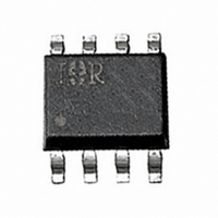
MOSFET N-CH 30V 6.5A 8-SOIC

IRF7353D2TRPBF

Manufacturer Part Number
IRF7353D2TRPBF
Description
MOSFET N-CH 30V 6.5A 8-SOIC
Manufacturer
International Rectifier
Series
FETKY™r
Datasheet

Specifications of IRF7353D2TRPBF

Fet Type
MOSFET N-Channel, Metal Oxide
Fet Feature
Diode (Isolated)
Rds On (max) @ Id, Vgs
29 mOhm @ 5.8A, 10V
Drain To Source Voltage (vdss)
30V
Current - Continuous Drain (id) @ 25° C
6.5A
Vgs(th) (max) @ Id
1V @ 250µA
Gate Charge (qg) @ Vgs
33nC @ 10V
Input Capacitance (ciss) @ Vds
650pF @ 25V
Power - Max
2W
Mounting Type
Surface Mount
Package / Case
8-SOIC (3.9mm Width)
Transistor Polarity
N-Channel
Resistance Drain-source Rds (on)
46 mOhms
Drain-source Breakdown Voltage
30 V
Gate-source Breakdown Voltage
20 V
Continuous Drain Current
6.5 A
Power Dissipation
2 W
Mounting Style
SMD/SMT
Gate Charge Qg
22 nC
Lead Free Status / RoHS Status
Lead free / RoHS Compliant
Other names
IRF7353D2PBFTR
IRF7353D2TRPBF
IRF7353D2TRPBFTR
Description
The FETKY™ family of Co-Pack HEXFET
diodes offers the designer an innovative, board space saving solution for
switching regulator and power management applications. Generation 5
HEXFET power MOSFETs utilize advanced processing techniques to
achieve extremely low on-resistance per silicon area. Combinining this
technology with International Rectifier's low forward drop Schottky rectifiers
results in an extremely efficient device suitable for use in a wide variety of
portable electronics applications.
The SO-8 has been modified through a customized leadframe for enhanced
thermal characteristics. The SO-8 package is designed for vapor phase,
infrared or wave soldering techniques.
Absolute Maximum Ratings (T
Thermal Resistance Ratings
Notes:
À
Á
Â
Ã
… †
www.irf.com
l
l
l
l
l
l
l
Parameter
R
Parameter
I
I
I
P
P
V
dv/dt
T
D
D
DM
θJA
D
D
GS
J,
Repetitive rating; pulse width limited by maximum junction temperature (see figure 9)
Starting T
I
Pulse width ≤ 300µs; duty cycle ≤ 2%
Surface mounted on FR-4 board, t ≤ 10sec
Lead-Free
Co-Pack HEXFET
Schottky Diode
Ideal For Buck Regulator Applications
N-Channel HEXFET power MOSFET
Low V
Generation 5 Technology
SO-8 Footprint
@ T
@ T
SD
T
@T
@T
STG
≤ 4.0A, di/dt ≤ 74A/µs, V
A
A
A
A
= 25°C
= 70°C
= 25°C
= 70°C
F
J
= 25°C, L = 10mH, R
Schottky Rectifier
®
DD
Power MOSFET and
Continuous Drain Current Ã
Pulsed Drain Current À
Power Dissipation Ã
Linear Derating Factor
Gate-to-Source Voltage
Peak Diode Recovery dv/dt Á
Junction and Storage Temperature Range
Junction-to-Ambient …
≤ V
G
(BR)DSS
= 25Ω, I
A
, T
®
= 25°C unless otherwise noted)
AS
J
Power MOSFETs and Schottky
≤ 150°C
= 4.0A
G
A
S
A
FETKY
1
2
3
4
Top View
IRF7353D2PbF
ä
MOSFET / Schottky Diode
8
6
5
7
-55 to +150
Maximum
K
± 20
K
D
D
Maximum
-5.0
6.5
5.2
2.0
1.3
52
16
62.5
Schottky V
R
DS(on)
V
DSS
PD- 95215A
SO-8
= 0.029Ω
= 30V
F
= 0.52V
Units
mW/°C
°C/W
Units
V/ns
10/8/04
°C
W
A
V
1

Related parts for IRF7353D2TRPBF

IRF7353D2TRPBF Summary of contents

Page 1

... Generation 5 HEXFET power MOSFETs utilize advanced processing techniques to achieve extremely low on-resistance per silicon area. Combinining this technology with International Rectifier's low forward drop Schottky rectifiers results in an extremely efficient device suitable for use in a wide variety of portable electronics applications. ...

Page 2

... Schottky Diode Electrical Specifications Parameter V Max. Forward voltage drop FM I Max. Reverse Leakage current rm C Max. Junction Capacitance t dv/dt Max. Voltage Rate of Charge ( HEXFET is the reg. TM for International Rectifier Power MOSFET 25°C (unless otherwise specified) J Min. Typ. Max. Units Conditions 30 — — 0V — ...

Page 3

Power MOSFET Characteristics 100 VGS TOP 15V 10V 7.0V 5.5V 4.5V 4.0V 3.5V BOTTOM 3.0V 10 20µs PULSE WIDTH T = 25° 0 Drain-to-Source Voltage (V) DS Fig 1. Typical Output Characteristics 100 T = ...

Page 4

IRF7353D2PbF 0.040 V = 4.5V GS 0.036 0.032 0.028 0.024 V GS 0.020 Drain Current (A) D Fig 5. Typical On-Resistance Vs. Drain Current 1200 1MHz ...

Page 5

Power MOSFET Characteristics 100 D = 0.50 0.20 10 0.10 0.05 0.02 0.01 1 SINGLE PULSE (THERMAL RESPONSE) 0.1 0.0001 0.001 Fig 9. Maximum Effective Transient Thermal Impedance, Junction-to-Ambient 100 10 1 www.irf.com 0.01 0 Rectangular Pulse Duration ...

Page 6

IRF7353D2PbF Schottky Diode Characteristics 100 10 1 0.1 0.0 0.2 0.4 0.6 Forward Voltage Drop - V Forward Voltage Drop - V Fig Typical Forward Voltage Drop Characteristics 6 100 10 1 0.1 0. 150°C J ...

Page 7

SO-8 (Fetky) Package Outline 0.25 [.010 NOT DIMENSIONING & TOLERANCING PER AS ME Y14.5M-1994. 2. ...

Page 8

IRF7353D2PbF SO-8 (Fetky) Tape and Reel TERMINAL NUMBER 1 8.1 ( .318 ) 7.9 ( .312 ) NOTES: 1. CONTROLLING DIMENSION : MILLIMETER. 2. ALL DIMENSIONS ARE SHOWN IN MILLIMETERS(INCHES). 3. OUTLINE CONFORMS TO EIA-481 & EIA-541. NOTES : 1. ...

Related keywords