PSMN2R2-40PS,127 NXP Semiconductors, PSMN2R2-40PS,127 Datasheet - Page 3
PSMN2R2-40PS,127
Manufacturer Part Number
PSMN2R2-40PS,127
Description
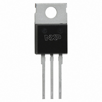
MOSFET N-CH 40V 100A TO-220AB3
Manufacturer
NXP Semiconductors
Datasheet
1.PSMN2R2-40PS127.pdf
(13 pages)
Specifications of PSMN2R2-40PS,127
Package / Case
TO-220AB-3
Fet Type
MOSFET N-Channel, Metal Oxide
Fet Feature
Standard
Rds On (max) @ Id, Vgs
2.1 mOhm @ 25A, 10V
Drain To Source Voltage (vdss)
40V
Current - Continuous Drain (id) @ 25° C
100A
Vgs(th) (max) @ Id
4V @ 1mA
Gate Charge (qg) @ Vgs
130nC @ 10V
Input Capacitance (ciss) @ Vds
8423pF @ 20V
Power - Max
306W
Mounting Type
Through Hole
Transistor Polarity
N-Channel
Resistance Drain-source Rds (on)
1.75 mOhms
Drain-source Breakdown Voltage
40 V
Continuous Drain Current
100 A
Power Dissipation
306 W
Mounting Style
Through Hole
Lead Free Status / RoHS Status
Lead free / RoHS Compliant
Lead Free Status / RoHS Status
Lead free / RoHS Compliant, Lead free / RoHS Compliant
Other names
568-4898-5
934063915127
934063915127


NXP Semiconductors
Table 4.
In accordance with the Absolute Maximum Rating System (IEC 60134).
PSMN2R2-40PS_2
Product data sheet
Symbol
Source-drain diode
I
I
Avalanche ruggedness
E
S
SM
Fig 1.
DS(AL)S
(A)
I
D
300
250
200
150
100
50
0
function of mounting base temperature
Normalized continuous drain current as a
0
Limiting values
Parameter
source current
peak source current
non-repetitive
drain-source avalanche
energy
50
(1)
…continued
100
Conditions
T
t
V
unclamped; R
p
mb
150
GS
≤ 10 µs; pulsed; T
= 25 °C
= 10 V; T
T
003aad125
mb
(°C)
Rev. 02 — 28 September 2009
200
j(init)
GS
= 50 Ω
= 25 °C; I
mb
= 25 °C
Fig 2.
D
= 100 A; V
P
(%)
N-channel 40 V 2.1 mΩ standard level MOSFET
der
120
80
40
0
function of mounting base temperature
Normalized total power dissipation as a
0
sup
≤ 40 V;
50
PSMN2R2-40PS
100
Min
-
-
-
150
© NXP B.V. 2009. All rights reserved.
T
mb
Max
100
962
1.24
03aa16
(°C)
200
Unit
A
A
J
3 of 13
Related parts for PSMN2R2-40PS,127
Image
Part Number
Description
Manufacturer
Datasheet
Request
R

Part Number:
Description:
MOSFET Std N-chanMOSFET
Manufacturer:
NXP Semiconductors
Datasheet:

Part Number:
Description:
MOSFET Power N-Ch 25V 2.4 mOhms
Manufacturer:
NXP Semiconductors
Datasheet:

Part Number:
Description:
Logic level enhancement mode N-channel MOSFET in LFPAK package
Manufacturer:
NXP Semiconductors
Datasheet:
Part Number:
Description:
Logic level enhancement mode N-channel MOSFET in LFPAK package
Manufacturer:
NXP Semiconductors
Datasheet:

Part Number:
Description:
Standard level N-channel MOSFET in TO220 package qualified to 175 �C
Manufacturer:
NXP Semiconductors
Datasheet:
Part Number:
Description:
MOSFET Power N-Ch 30V 2.15mOhms
Manufacturer:
NXP Semiconductors
Datasheet:
Part Number:
Description:
NXP Semiconductors designed the LPC2420/2460 microcontroller around a 16-bit/32-bitARM7TDMI-S CPU core with real-time debug interfaces that include both JTAG andembedded trace
Manufacturer:
NXP Semiconductors
Datasheet:

Part Number:
Description:
NXP Semiconductors designed the LPC2458 microcontroller around a 16-bit/32-bitARM7TDMI-S CPU core with real-time debug interfaces that include both JTAG andembedded trace
Manufacturer:
NXP Semiconductors
Datasheet:
Part Number:
Description:
NXP Semiconductors designed the LPC2468 microcontroller around a 16-bit/32-bitARM7TDMI-S CPU core with real-time debug interfaces that include both JTAG andembedded trace
Manufacturer:
NXP Semiconductors
Datasheet:
Part Number:
Description:
NXP Semiconductors designed the LPC2470 microcontroller, powered by theARM7TDMI-S core, to be a highly integrated microcontroller for a wide range ofapplications that require advanced communications and high quality graphic displays
Manufacturer:
NXP Semiconductors
Datasheet:
Part Number:
Description:
NXP Semiconductors designed the LPC2478 microcontroller, powered by theARM7TDMI-S core, to be a highly integrated microcontroller for a wide range ofapplications that require advanced communications and high quality graphic displays
Manufacturer:
NXP Semiconductors
Datasheet:
Part Number:
Description:
The Philips Semiconductors XA (eXtended Architecture) family of 16-bit single-chip microcontrollers is powerful enough to easily handle the requirements of high performance embedded applications, yet inexpensive enough to compete in the market for hi
Manufacturer:
NXP Semiconductors
Datasheet:
Part Number:
Description:
The XA-S3 device is a member of Philips Semiconductors? XA(eXtended Architecture) family of high performance 16-bitsingle-chip microcontrollers
Manufacturer:
NXP Semiconductors
Datasheet:

Part Number:
Description:
The NXP BlueStreak LH75401/LH75411 family consists of two low-cost 16/32-bit System-on-Chip (SoC) devices
Manufacturer:
NXP Semiconductors
Datasheet: