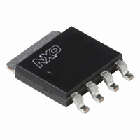
PSMN9R0-30YL,115 NXP Semiconductors, PSMN9R0-30YL,115 Datasheet - Page 6

PSMN9R0-30YL,115
Manufacturer Part Number
PSMN9R0-30YL,115
Description
MOSFET N-CH 30V 55A LFPAK
Manufacturer
NXP Semiconductors
Datasheet
1.PSMN9R0-30YL115.pdf
(14 pages)
Specifications of PSMN9R0-30YL,115
Package / Case
LFPak-4
Fet Type
MOSFET N-Channel, Metal Oxide
Fet Feature
Logic Level Gate
Rds On (max) @ Id, Vgs
8 mOhm @ 15A, 10V
Drain To Source Voltage (vdss)
30V
Current - Continuous Drain (id) @ 25° C
55A
Vgs(th) (max) @ Id
2.15V @ 1mA
Gate Charge (qg) @ Vgs
17.8nC @ 10V
Input Capacitance (ciss) @ Vds
1006pF @ 12V
Power - Max
46W
Mounting Type
Surface Mount
Minimum Operating Temperature
- 55 C
Configuration
Single Triple Source
Transistor Polarity
N-Channel
Resistance Drain-source Rds (on)
9 mOhms
Drain-source Breakdown Voltage
30 V
Gate-source Breakdown Voltage
20 V
Continuous Drain Current
61 A
Power Dissipation
46 W
Maximum Operating Temperature
+ 175 C
Mounting Style
SMD/SMT
Lead Free Status / RoHS Status
Lead free / RoHS Compliant
Lead Free Status / RoHS Status
Lead free / RoHS Compliant, Lead free / RoHS Compliant
Other names
568-4687-2
934063067115
PSMN9R0-30YL T/R
934063067115
PSMN9R0-30YL T/R
NXP Semiconductors
Table 6.
Tested to JEDEC standards where applicable.
PSMN9R0-30YL
Product data sheet
Symbol
Source-drain diode
V
t
Q
rr
Fig 5.
Fig 7.
SD
r
(S)
g
(A)
80
60
40
20
60
50
40
30
I
fs
D
0
function of drain-source voltage; typical values
drain current; typical values
Output characteristics: drain current as a
Forward transconductance as a function of
0
5
10
Characteristics
4.5
3.5
Parameter
source-drain voltage
reverse recovery time
recovered charge
10
2
15
4
…continued
20
6
V
GS
Conditions
I
see
I
V
25
All information provided in this document is subject to legal disclaimers.
S
S
8
DS
003aac534
003aac539
(V) = 3
= 25 A; V
= 20 A; dI
V
I
DS
D
Figure 17
= 20 V
(A)
2.8
2.6
2.4
2.2
(V)
10
30
Rev. 04 — 9 March 2011
GS
S
/dt = -100 A/µs; V
= 0 V; T
N-channel 30 V 8 mΩ logic level MOSFET in LFPAK
Fig 6.
Fig 8.
j
= 25 °C;
R
(mΩ)
(A)
DSon
I
14
12
10
D
60
40
20
8
6
4
0
function of gate-source voltage; typical values
of drain current; typical values
Transfer characteristics: drain current as a
Drain-source on-state resistance as a function
GS
0
0
= 0 V;
V
GS
(V) = 3.5
1
T
j
20
= 150 °C
PSMN9R0-30YL
Min
-
-
-
2
40
25 °C
Typ
0.88
26
16
3
7.5
4.5
© NXP B.V. 2011. All rights reserved.
10
I
D
V
003aac535
003aac546
(A)
GS
Max
1.2
-
-
(V)
60
4
Unit
V
ns
nC
6 of 14


