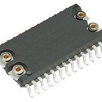
M48T86MH1 STMicroelectronics, M48T86MH1 Datasheet - Page 9

M48T86MH1
Manufacturer Part Number
M48T86MH1
Description
Real Time Clock USE 511-M48T86MH1E
Manufacturer
STMicroelectronics
Datasheet
1.M48T86MH1.pdf
(36 pages)
Specifications of M48T86MH1
Function
Clock, Calendar, Interrupt, Alarm
Rtc Memory Size
128 B
Supply Voltage (max)
5.5 V
Supply Voltage (min)
4.5 V
Maximum Operating Temperature
+ 70 C
Minimum Operating Temperature
0 C
Mounting Style
SMD/SMT
Rtc Bus Interface
Multiplexed
Package / Case
SO-28
Time Format
HH:MM:SS, Binary
Date Format
DW:DM:M:Y, Binary
Lead Free Status / RoHS Status
Lead free / RoHS Compliant
Available stocks
Company
Part Number
Manufacturer
Quantity
Price
Company:
Part Number:
M48T86MH1
Manufacturer:
CARTYS
Quantity:
2 585
Part Number:
M48T86MH1
Manufacturer:
ST
Quantity:
20 000
M48T86
2
2.1
2.1.1
2.1.2
2.1.3
2.1.4
Operation
The M48T86 clock is driven by a quartz-controlled oscillator with a nominal frequency of
32,768 Hz. The devices are tested not to exceed 23 ppm (parts per million) oscillator
frequency error at 25°C, which equates to approximately ±1 minute per month. Automatic
deselection of the device ensures the data integrity is not compromised should V
below specified power-fail deselect voltage (V
automatic deselection of the device remains in effect upon power up for a period of 200ms
(max) after V
down chain is not reset. This allows sufficient time for V
clock a wake-up period so that a valid system reset can be established.
The block diagram in
functions of the M48T86.
Signal description
V
DC power is provided to the device on these pins.The M48T86 uses a 5 V V
SQW (square wave output)
During normal operation (e.g., valid V
taps. The frequency of the SQW pin can be changed by programming Register A as shown
in
(Register B; Bit 3). The SQW signal is not available when V
AD0-AD7 (multiplexed bidirectional address/data bus)
The M48T86 provides a multiplexed bus in which address and data information share the
same signal path. The bus cycle consists of two stages; first the address is latched, followed
by the data. Address/Data multiplexing does not slow the access time of the M48T86,
because the bus change from address to data occurs during the internal RAM access time.
Addresses must be valid prior to the falling edge of AS (see
time the M48T86 latches the address present on AD0-AD7. Valid WRITE data must be
present and held stable during the latter portion of the R/W pulse (see
In a READ cycle, the M48T86 outputs 8 bits of data during the latter portion of the DS pulse.
The READ cycle is terminated and the bus returns to a high impedance state upon a high
transition on R/W.
AS (address strobe input)
A positive going pulse on the Address Strobe (AS) input serves to demultiplex the bus. The
falling edge of AS causes the address present on AD0-AD7 to be latched within the
M48T86.
CC
Table 4 on page
, V
SS
CC
rises above V
18. The SQW signal can be turned on and off using the SQWE bit
Figure 4 on page 8
PFD
, provided that the real-time clock is running and the count-
CC
), the SQW pin can output a signal from one of 13
shows the pin connections and the major internal
PFD
) levels (see
CC
to stabilize and gives the system
CC
Figure 5 on page
Figure 14 on page
is less than V
Figure 6 on page
CC
PFD
11), at which
.
.
CC
Operation
27). The
fall
11).
9/36


