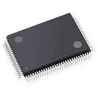
ISPPAC-CLK5620V-01TN100I Lattice, ISPPAC-CLK5620V-01TN100I Datasheet - Page 17

ISPPAC-CLK5620V-01TN100I
Manufacturer Part Number
ISPPAC-CLK5620V-01TN100I
Description
Clock Drivers & Distribution PROGRAMMABLE ZERO DELAY CL GEN
Manufacturer
Lattice
Type
Zero Delay Programmable PLL Clock Generatorr
Datasheet
1.ISPPAC-CLK5620V-01TN100C.pdf
(49 pages)
Specifications of ISPPAC-CLK5620V-01TN100I
Max Input Freq
320 MHz
Minimum Operating Temperature
- 40 C
Mounting Style
SMD/SMT
Supply Voltage (max)
3.6 V
Supply Voltage (min)
3 V
Maximum Operating Temperature
+ 85 C
Package / Case
TQFP-100
Lead Free Status / RoHS Status
Lead free / RoHS Compliant
Available stocks
Company
Part Number
Manufacturer
Quantity
Price
Company:
Part Number:
ISPPAC-CLK5620V-01TN100I
Manufacturer:
Lattice Semiconductor Corporation
Quantity:
10 000
Lattice Semiconductor
Table 2. Filter Settings for Minimizing Cycle-Cycle and Period Jitter
Table 3. Filter Settings for Optimizing Overall Jitter (Recommended)
Note that the choice of loop filter parameters can have significant effects on settling time, output jitter, and whether
the PLL will be fundamentally stable and be able to lock to an incoming signal. The values recommended in Table 2
and Table 3 were chosen to provide maximum loop stability while still providing exceptional jitter performance.
Please note that when the skew mode is set to ‘coarse’, the effective value of NxV must be considered to have dou-
bled. Refer to the section titled ‘Coarse Skew Mode’ on page 30 for further details.
The PLL’s loop bandwidth is a function of both the divider configuration and the loop filter settings. Figure 12 shows
the loop bandwidth as a function of the total feedback division ratio (N x V
in this plot, the PLL loop filter was set to the corresponding value recommended in Table 2. The use of non-recom-
mended loop filter settings may result in significantly different bandwidths for a given NxV divider setting.
Note: Do not use this setting if phase jitter performance opti-
mization is required.
N x V
N x V
12 to 14
18 to 20
24 to 26
32 to 64
16 to 22
24 to 52
54 to 62
8 to 14
2 to 8
4 to 6
10
16
22
28
30
2
FBK
FBK
I (µA)
I (µA)
17
11
13
15
17
19
21
22
17
33
55
55
55
55
5
7
9
R (kΩ)
R (kΩ)
2.3
2.3
2.3
2.3
2.3
2.3
2.3
2.3
2.3
2.3
2.3
2.3
2.3
3.7
5.1
7.9
ispClock5600 Family Data Sheet
FBK
). For each NxV feedback divider point


