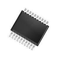
TDA8542TSDK-T NXP Semiconductors, TDA8542TSDK-T Datasheet - Page 7

TDA8542TSDK-T
Manufacturer Part Number
TDA8542TSDK-T
Description
Audio Amplifiers 2X1.5W BTL PWR AMP
Manufacturer
NXP Semiconductors
Datasheet
1.TDA8542TSN1112.pdf
(20 pages)
Specifications of TDA8542TSDK-T
Product
Class-AB
Output Power
1.2 W
Available Set Gain
30 dB
Thd Plus Noise
0.15 %
Operating Supply Voltage
5 V
Supply Current
15 mA
Maximum Power Dissipation
1120 mW
Maximum Operating Temperature
+ 85 C
Mounting Style
SMD/SMT
Audio Load Resistance
16 Ohms
Input Bias Current (max)
500 nA
Input Signal Type
Differential or Single
Minimum Operating Temperature
- 40 C
Output Signal Type
Differential, Single
Supply Type
Single
Supply Voltage (max)
18 V
Supply Voltage (min)
2.2 V
Output Type
2-Channel Stereo
Package / Case
SSOP-20
Lead Free Status / RoHS Status
Lead free / RoHS Compliant
Other names
TDA8542TS/N1,118
NXP Semiconductors
AC CHARACTERISTICS
V
Notes
1. Gain of the amplifier is
2. The noise output voltage is measured at the output in a frequency range from 20 Hz to 20 kHz (unweighted), with a
3. Supply voltage ripple rejection is measured at the output, with a source impedance of R
4. Supply voltage ripple rejection is measured at the output, with a source impedance of R
5. Output voltage in mute position is measured with a 1 V (RMS) input voltage in a bandwidth of 20 kHz, so including
1998 Mar 25
P
THD
G
Z
V
SVRR
V
α
CC
SYMBOL
i(dif)
cs
o
n(o)
o(mute)
2 × 0.7 W BTL audio amplifier
v(cl)
source impedance of R
The ripple voltage is a sine wave with a frequency of 1 kHz and an amplitude of 100 mV (RMS), which is applied to
the positive supply rail.
The ripple voltage is a sine wave with a frequency between 100 Hz and 20 kHz and an amplitude of 100 mV (RMS),
which is applied to the positive supply rail.
noise.
= 5 V; T
amb
output power
total harmonic distortion
closed-loop voltage gain
differential input impedance
noise output voltage
supply voltage ripple rejection
output voltage in mute condition
channel separation
= 25 °C; R
PARAMETER
L
S
2
= 8 Ω; f = 1 kHz; V
= 0 Ω at the input.
×
R2
------ -
R1
in test circuit of Fig.3.
MODE
at V
at V
P
note 1
note 2
note 3
note 4
note 5
o
THD = 10%; R
THD = 10%; R
THD = 0.5%; R
THD = 0.5%; R
THD = 10%; R
THD = 10%; R
THD = 0.5%; R
THD = 0.5%; R
= 0.4 W
= 0 V; measured in test circuit Fig.3; unless otherwise specified.
CC
CC
= 5 V
= 3.3 V
CONDITIONS
7
L
L
L
L
L
L
L
L
= 8 Ω
= 16 Ω
= 4 Ω
= 8 Ω
= 8 Ω
= 16 Ω
= 4 Ω
= 8 Ω
−
−
−
−
−
−
−
−
−
6
−
−
50
40
−
40
MIN.
1.2
0.70
0.9
0.5
0.65
0.55
0.45
0.38
0.15
−
100
−
−
−
−
−
S
S
TYP.
= 0 Ω at the input.
= 0 Ω at the input.
TDA8542TS
Product specification
−
−
−
−
−
−
−
−
0.3
30
−
100
−
−
200
−
MAX.
W
W
W
W
W
W
W
W
%
dB
kΩ
μV
dB
dB
μV
dB
UNIT


