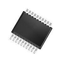
TDA8542TSDK-T NXP Semiconductors, TDA8542TSDK-T Datasheet - Page 5

TDA8542TSDK-T
Manufacturer Part Number
TDA8542TSDK-T
Description
Audio Amplifiers 2X1.5W BTL PWR AMP
Manufacturer
NXP Semiconductors
Datasheet
1.TDA8542TSN1112.pdf
(20 pages)
Specifications of TDA8542TSDK-T
Product
Class-AB
Output Power
1.2 W
Available Set Gain
30 dB
Thd Plus Noise
0.15 %
Operating Supply Voltage
5 V
Supply Current
15 mA
Maximum Power Dissipation
1120 mW
Maximum Operating Temperature
+ 85 C
Mounting Style
SMD/SMT
Audio Load Resistance
16 Ohms
Input Bias Current (max)
500 nA
Input Signal Type
Differential or Single
Minimum Operating Temperature
- 40 C
Output Signal Type
Differential, Single
Supply Type
Single
Supply Voltage (max)
18 V
Supply Voltage (min)
2.2 V
Output Type
2-Channel Stereo
Package / Case
SSOP-20
Lead Free Status / RoHS Status
Lead free / RoHS Compliant
Other names
TDA8542TS/N1,118
NXP Semiconductors
Headphone connection
A headphone can be connected to the amplifier using two
coupling capacitors for each channel. The common
GND pin of the headphone is connected to the ground of
the amplifier (see Fig.13). In this case the BTL/SE pin must
be either at a logic HIGH level or not connected at all.
The two coupling capacitors can be omitted if it is allowed
to connect the common GND pin of the headphone jack
LIMITING VALUES
In accordance with the Absolute Maximum Rating System (IEC 134).
QUALITY SPECIFICATION
In accordance with “SNW-FQ-611-E”.
THERMAL CHARACTERISTICS
Note
1. See Section “Thermal design considerations”.
Table 1 Maximum ambient temperature at different conditions
Note
1. See Section “Thermal design considerations”.
1998 Mar 25
V
V
I
T
T
V
P
R
SYMBOL
SYMBOL
ORM
stg
amb
CC
I
sc
tot
2 × 0.7 W BTL audio amplifier
th(j-a)
V
(V)
3.3
3.3
5
5
CC
supply voltage
input voltage
repetitive peak output current
storage temperature
operating ambient temperature
AC and DC short-circuit safe voltage
total power dissipation
thermal resistance from junction to ambient
PARAMETER
PARAMETER
(Ω)
R
16
4
8
8
L
2 × 0.65
2 × 0.55
2 × 0.70
2 × 1.2
(W)
P
5
o
not to ground, but to a voltage level of
the application diagram. In this case the BTL/SE pin must
be either at a logic LOW level or connected to ground.
If the BTL/SE pin is at a LOW level, the power amplifier for
the positive loudspeaker terminal is always in mute
condition.
operating
non-operating
CONDITIONS
in free air
CONDITIONS
CONTINUOUS SINE WAVE DRIVEN
P
1.12
0.60
1.33
0.80
(W)
max
−0.3
−0.3
−
−55
−40
−
−
MIN.
+18
V
1
+150
+85
10
1.12
VALUE
CC
TDA8542TS
Product specification
MAX.
110
1
⁄
2
V
+ 0.3 V
(1)
CC
T
amb(max)
. See Fig.4 for
27
(°C)
−
84
62
(1)
(1)
V
A
°C
°C
V
W
UNIT
UNIT
K/W


