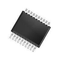
TDA8542TSDK-T NXP Semiconductors, TDA8542TSDK-T Datasheet - Page 4

TDA8542TSDK-T
Manufacturer Part Number
TDA8542TSDK-T
Description
Audio Amplifiers 2X1.5W BTL PWR AMP
Manufacturer
NXP Semiconductors
Datasheet
1.TDA8542TSN1112.pdf
(20 pages)
Specifications of TDA8542TSDK-T
Product
Class-AB
Output Power
1.2 W
Available Set Gain
30 dB
Thd Plus Noise
0.15 %
Operating Supply Voltage
5 V
Supply Current
15 mA
Maximum Power Dissipation
1120 mW
Maximum Operating Temperature
+ 85 C
Mounting Style
SMD/SMT
Audio Load Resistance
16 Ohms
Input Bias Current (max)
500 nA
Input Signal Type
Differential or Single
Minimum Operating Temperature
- 40 C
Output Signal Type
Differential, Single
Supply Type
Single
Supply Voltage (max)
18 V
Supply Voltage (min)
2.2 V
Output Type
2-Channel Stereo
Package / Case
SSOP-20
Lead Free Status / RoHS Status
Lead free / RoHS Compliant
Other names
TDA8542TS/N1,118
NXP Semiconductors
PINNING
FUNCTIONAL DESCRIPTION
The TDA8542TS is a 2 × 0.7 W BTL audio power amplifier
capable of delivering 2 × 0.7 W output power to a 16 Ω
load at THD = 10% using a 5 V power supply. Using the
MODE pin the device can be switched to standby and
mute condition. The device is protected by an internal
thermal shutdown protection mechanism. The gain can be
set within a range from 6 to 30 dB by external feedback
resistors.
Power amplifier
The power amplifier is a Bridge-Tied Load (BTL) amplifier
with a complementary PNP-NPN output stage.
The voltage loss on the positive supply line is the
saturation voltage of a PNP power transistor, on the
negative side the saturation voltage of a NPN power
1998 Mar 25
LGND
n.c.
OUTL+
MODE
SVR
BTL/SE
n.c.
OUTR+
n.c.
RGND
V
n.c.
OUTR−
INR−
INR+
INL+
INL−
OUTL−
n.c.
V
CCR
CCL
2 × 0.7 W BTL audio amplifier
SYMBOL
PIN
10
12
13
14
15
16
17
18
19
20
11
1
2
3
4
5
6
7
8
9
ground, left channel
not connected
positive loudspeaker terminal, left
channel
operating mode select (standby,
mute, operating)
half supply voltage, decoupling
ripple rejection
BTL loudspeaker or SE
headphone operation
not connected
positive loudspeaker terminal,
right channel
not connected
ground, right channel
supply voltage, right channel
not connected
negative loudspeaker terminal,
right channel
negative input, right channel
positive input, right channel
positive input, left channel
negative input, left channel
negative loudspeaker terminal,
left channel
not connected
supply voltage, left channel
DESCRIPTION
4
transistor. The total voltage loss is <1 V and with a 5 V
supply voltage and with a 16 Ω loudspeaker an output
power of 0.7 W can be delivered.
Mode select pin
The device is in the standby mode (with a very low current
consumption) if the voltage at the MODE pin is
>(V
level of less than 0.5 V the amplifier is fully operational.
In the range between 1.5 V and V
is in mute condition. The mute condition is useful to
suppress plop noise at the output caused by charging of
the input capacitor.
handbook, halfpage
CC
− 0.5 V), or if this pin is floating. At a MODE voltage
BTL/SE
OUTR
OUTL
MODE
RGND
LGND
SVR
n.c.
n.c.
n.c.
Fig.2 Pin configuration.
10
1
2
3
4
5
6
7
8
9
TDA8542TS
MBK453
CC
20
19
18
17
16
15
14
13
12
11
TDA8542TS
Product specification
− 1.5 V the amplifier
V CCL
n.c.
OUTL
INL
INL
INR
INR
OUTR
n.c.
V CCR


