NTJD4158CT1G ON Semiconductor, NTJD4158CT1G Datasheet - Page 2
NTJD4158CT1G
Manufacturer Part Number
NTJD4158CT1G
Description
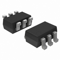
MOSFET N/P-CHAN COMPL SOT-363
Manufacturer
ON Semiconductor
Datasheet
1.NTJD4158CT2G.pdf
(7 pages)
Specifications of NTJD4158CT1G
Fet Type
N and P-Channel
Fet Feature
Logic Level Gate
Rds On (max) @ Id, Vgs
1.5 Ohm @ 10mA, 4.5V
Drain To Source Voltage (vdss)
30V, 20V
Current - Continuous Drain (id) @ 25° C
250mA, 880mA
Vgs(th) (max) @ Id
1.5V @ 100µA
Gate Charge (qg) @ Vgs
1.5nC @ 5V
Input Capacitance (ciss) @ Vds
33pF @ 5V
Power - Max
270mW
Mounting Type
Surface Mount
Package / Case
SC-70-6, SC-88, SOT-363
Lead Free Status / RoHS Status
Lead free / RoHS Compliant
Other names
NTJD4158CT1G
NTJD4158CT1GOSTR
NTJD4158CT1GOSTR
Available stocks
Company
Part Number
Manufacturer
Quantity
Price
Company:

Part Number:
NTJD4158CT1G
Manufacturer:
ON
Quantity:
30 000
Part Number:
NTJD4158CT1G
Manufacturer:
ON/安森美
Quantity:
20 000


2. Pulse Test: pulse width ≤ 300 ms, duty cycle ≤ 2%.
3. Switching characteristics are independent of operating junction temperatures.
ELECTRICAL CHARACTERISTICS
OFF CHARACTERISTICS (Note 3)
Drain−to−Source
Drain−to−Source Breakdown
Zero Gate Voltage Drain Current
Gate−to−Source Leakage Current
ON CHARACTERISTICS (Note 2)
Gate Threshold Voltage
Negative Gate Threshold
Drain−to−Source On Resistance
Forward Transconductance
CHARGES, CAPACITANCES AND GATE RESISTANCE
Input Capacitance
Output Capacitance
Reverse Transfer Capacitance
Total Gate Charge
Threshold Gate Charge
Gate−to−Source Charge
Gate−to−Drain Charge
SWITCHING CHARACTERISTICS (Note 3)
Turn−On Delay Time
Rise Time
Turn−Off Delay Time
Fall Time
Turn−On Delay Time
Rise Time
Turn−Off Delay Time
Fall Time
DRAIN−SOURCE DIODE CHARACTERISTICS
Forward Diode Voltage
Reverse Recovery Time
Breakdown Voltage
Voltage Temperature Coefficient
Temperature Coefficient
Parameter
V
V
V
Symbol
V
Q
R
Q
(BR)DSS
t
t
(BR)DSS
GS(TH)
C
C
t
t
d(OFF)
d(OFF)
GS(TH)
I
I
C
G(TOT)
Q
Q
d(ON)
d(ON)
DS(on)
V
g
DSS
GSS
G(TH)
t
(T
T
T
OSS
RSS
RR
FS
ISS
t
t
t
t
SD
GS
GD
r
f
r
f
J
J
J
= 25°C unless otherwise noted)
/
/
N/P
N
P
N
P
N
P
N
P
N
P
N
P
N
P
N
P
N
P
N
P
N
P
N
P
N
P
N
P
N
P
N
P
N
P
N
P
N
P
N
P
N
P
http://onsemi.com
V
V
GS
GS
V
V
V
V
V
V
V
V
V
f = 1 MHz, V
V
GS
GS
GS
GS
GS
GS
GS
GS
GS
= 0 V, d
V
V
V
V
GS
= 0 V, d
GS
GS
GS
GS
= 0 V, V
= 0 V, V
= −4.5 V, V
= −4.5 V, V
= −4.5 V, V
= −4.5 V, V
= 0 V, V
= 0 V, V
= 0 V, T
= 0 V, T
V
V
V
V
V
V
2
V
= 5.0 V, V
= 5.0 V, V
= 5.0 V, V
= 5.0 V, V
GS
GS
V
GS
V
V
V
I
GS
GS
GS
DS
D
I
V
DS
D
GS
GS
DS
IS
IS
DS
= 250 mA, R
= V
= −4.5 V, V
= 0 V
= −0.5 A, R
= −4.5 V, I
= −2.5 V, I
= −10 V, I
= 4.5 V, V
/d
/d
Test Condition
DS
DS
= 0 V, V
= 4.5 V, I
= 2.5 V, I
= 3.0 V, I
J
DS
DS
= 0 V, V
GS
J
t
t
DS
= 125°C
= 100 A/ms
= 8.0 A/ms
= 25°C
= −16 V
= −16 V
DS
DS
DS
DS
= 30 V
= 30 V
= 0 V
DS
DS
DS
DS
= −10 V, I
= −10 V, I
= −10 V, I
= −10 V, I
= 24 V, I
= 24 V, I
= 24 V, I
= 24 V, I
GS
GS
D
DD
D
D
D
D
D
DD
G
= −0.88 A
G
= 10 mA
= −0.88 A
= 10 mA
= −0.71 A
= 10 mA
= −4.5 V
= 20 W
= 10 V
= 5.0 V,
= 50 W
= −10 V,
D
D
D
D
D
D
D
D
I
I
I
S
V
V
V
I
I
V
V
V
= 0.1 A
= −0.88 A
= 0.1 A
= −0.88 A
= 0.1 A
= −0.88 A
= 0.1 A
= −0.88 A
I
D
I
D
T
I
S
I
S
I
D
D
T
S
S
S
DS
DS
DS
= −0.48 mA
DS
DS
DS
J
= −250 mA
= −250 mA
= −0.48 A
= −0.48 A
J
= 250 mA
= 100 mA
= 10 mA
= 10 mA
= 10 mA
= 125°C
= 25°C
= −20 V
= −20 V
= −20 V
= 5.0 V
= 5.0 V
= 5.0 V
−0.45
Min
−20
0.8
30
0.215
0.345
−0.66
−9.0
−2.7
0.08
7.25
0.65
13.5
0.65
−0.8
0.45
12.4
TBD
Typ
155
0.5
0.5
1.2
3.2
1.0
1.5
3.0
0.9
2.2
0.2
0.2
0.3
0.5
0.2
5.8
6.5
3.5
33
20
19
25
18
15
66
56
78
0.260
0.500
Max
−1.2
225
1.0
1.0
1.0
1.0
1.5
1.5
2.5
1.5
3.5
0.7
33
32
40
12
30
Unit
mV/
mV/
mA
mA
nC
°C
°C
pF
ns
ns
W
V
V
S
V
Related parts for NTJD4158CT1G
Image
Part Number
Description
Manufacturer
Datasheet
Request
R

Part Number:
Description:
ON Semiconductor [VOLTAGE REGULATOR]
Manufacturer:
ON Semiconductor
Datasheet:
Part Number:
Description:
357-036-542-201 CARDEDGE 36POS DL .156 BLK LOPRO
Manufacturer:
ON Semiconductor
Datasheet:
Part Number:
Description:
357-036-542-201 CARDEDGE 36POS DL .156 BLK LOPRO
Manufacturer:
ON Semiconductor
Datasheet:
Part Number:
Description:
357-036-542-201 CARDEDGE 36POS DL .156 BLK LOPRO
Manufacturer:
ON Semiconductor
Datasheet:
Part Number:
Description:
357-036-542-201 CARDEDGE 36POS DL .156 BLK LOPRO
Manufacturer:
ON Semiconductor
Datasheet:
Part Number:
Description:
357-036-542-201 CARDEDGE 36POS DL .156 BLK LOPRO
Manufacturer:
ON Semiconductor
Datasheet:
Part Number:
Description:
357-036-542-201 CARDEDGE 36POS DL .156 BLK LOPRO
Manufacturer:
ON Semiconductor
Datasheet:
Part Number:
Description:
357-036-542-201 CARDEDGE 36POS DL .156 BLK LOPRO
Manufacturer:
ON Semiconductor
Datasheet:
Part Number:
Description:
357-036-542-201 CARDEDGE 36POS DL .156 BLK LOPRO
Manufacturer:
ON Semiconductor
Datasheet:
Part Number:
Description:
357-036-542-201 CARDEDGE 36POS DL .156 BLK LOPRO
Manufacturer:
ON Semiconductor
Datasheet:
Part Number:
Description:
357-036-542-201 CARDEDGE 36POS DL .156 BLK LOPRO
Manufacturer:
ON Semiconductor
Datasheet:
Part Number:
Description:
Manufacturer:
ON Semiconductor
Datasheet:
Part Number:
Description:
Manufacturer:
ON Semiconductor
Datasheet:
Part Number:
Description:
Manufacturer:
ON Semiconductor
Datasheet: