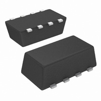
SI5509DC-T1-E3 Vishay, SI5509DC-T1-E3 Datasheet - Page 8

SI5509DC-T1-E3
Manufacturer Part Number
SI5509DC-T1-E3
Description
MOSFET N/P-CH 20V CHIPFET 1206-8
Manufacturer
Vishay
Series
TrenchFET®r
Specifications of SI5509DC-T1-E3
Fet Type
N and P-Channel
Fet Feature
Logic Level Gate
Rds On (max) @ Id, Vgs
52 mOhm @ 5A, 4.5V
Drain To Source Voltage (vdss)
20V
Current - Continuous Drain (id) @ 25° C
5A, 3.9A
Vgs(th) (max) @ Id
2V @ 250µA
Gate Charge (qg) @ Vgs
6.6nC @ 5V
Input Capacitance (ciss) @ Vds
455pF @ 10V
Power - Max
2.1W
Mounting Type
Surface Mount
Package / Case
1206-8 ChipFET™
Transistor Polarity
N And P Channel
Continuous Drain Current Id
5A
Drain Source Voltage Vds
20V
On Resistance Rds(on)
43mohm
Rds(on) Test Voltage Vgs
5V
Threshold Voltage Vgs Typ
2V
Configuration
Dual Dual Drain
Resistance Drain-source Rds (on)
0.052 Ohms
Drain-source Breakdown Voltage
20 V
Gate-source Breakdown Voltage
+/- 12 V
Continuous Drain Current
5 A, - 3.9 A
Power Dissipation
2.1 W
Maximum Operating Temperature
+ 150 C
Mounting Style
SMD/SMT
Minimum Operating Temperature
- 55 C
Lead Free Status / RoHS Status
Lead free / RoHS Compliant
Lead Free Status / RoHS Status
Lead free / RoHS Compliant, Lead free / RoHS Compliant
Other names
SI5509DC-T1-E3TR
Available stocks
Company
Part Number
Manufacturer
Quantity
Price
Si5509DC
Vishay Siliconix
P-CHANNEL TYPICAL CHARACTERISTICS 25 °C, unless otherwise noted
www.vishay.com
8
0.20
0.15
0.10
0.05
0.00
10
2
0
8
6
4
On-Resistance vs. Drain Current and Gate Voltage
5
4
3
2
1
0
0
0
0
I
D
= 3.9 A
V
GS
0.6
2
1
= 2.5 V
V
DS
Output Characteristics
- Drain-to-Source Voltage (V)
Q
I
D
g
V
- Drain Current (A)
- Total Gate Charge
Gate Charge
1.2
DS
4
2
= 10 V
V
GS
V
GS
= 5 V thru 3 V
V
GS
= 4.5 V
1.8
6
3
= 2 V
V
GS
V
V
GS
= 1.5 V
DS
= 2.5 V
2.4
= 16 V
8
4
3.0
10
5
100
600
500
400
300
200
0.8
0.6
1.6
1.4
1.2
1.0
5
4
3
2
1
0
0
- 50
0
0
C
On-Resistance vs. Junction Temperature
- 25
rss
0.5
C
4
V
oss
V
V
V
GS
DS
0
Transfer Characteristics
T
GS
GS
J
C
- Drain-to-Source Voltage (V)
T
- Gate-to-Source Voltage (V)
- Junction Temperature (°C)
iss
C
= 4.5 V, I
= 2.5 V, I
T
C
= 125 °C
25
= 25 °C
Capacitance
1.0
8
D
D
50
= 5 A
= 3.9 A
S10-0547-Rev. B, 08-Mar-10
Document Number: 73629
1.5
12
75
T
C
= - 55 °C
100
2.0
16
125
150
2.5
20


