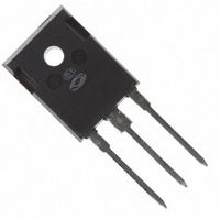
APT50GS60BRDQ2G Microsemi Power Products Group, APT50GS60BRDQ2G Datasheet

IGBT 600V 93A 415W TO247

APT50GS60BRDQ2G

Manufacturer Part Number
APT50GS60BRDQ2G
Description
IGBT 600V 93A 415W TO247
Manufacturer
Microsemi Power Products Group
Series
Thunderbolt IGBT®r
Datasheet

Specifications of APT50GS60BRDQ2G

Igbt Type
NPT
Voltage - Collector Emitter Breakdown (max)
600V
Vce(on) (max) @ Vge, Ic
3.15V @ 15V, 50A
Current - Collector (ic) (max)
93A
Power - Max
415W
Input Type
Standard
Mounting Type
Through Hole
Package / Case
TO-247
Lead Free Status / RoHS Status
Lead free / RoHS Compliant
Other names
APT50GS60BRDQ2GMI
APT50GS60BRDQ2GMI

Available stocks

Company
Part Number
Manufacturer
Quantity
Price
Company:
Part Number:
APT50GS60BRDQ2G
Quantity:
4 000
Features
• Fast Switching with low EMI
• Very Low E
• Short circuit rated
• Low Gate Charge
• Tight parameter distribution
• Easy paralleling
• RoHS Compliant
Absolute Maximum Ratings
Thermal and Mechanical Characteristics
T
Symbol
Symbol
The Thunderbolt HS
the Thunderbolt
switching losses enable operation at switching frequencies over 100kHz, approaching power MOSFET
performance but lower cost.
An extremely tight parameter distribution combined with a positive V
make it easy to parallel Thunderbolts HS
and oscillation immunity and low EMI. The short circuit duration rating of 10µs make these IGBT's
suitable for motor drive and inverter applications. Reliability is further enhanced by avalanche energy
ruggedness. Combi versions are packaged with a high speed, soft recovery DQ series diode.
Torque
SSOA
J
R
R
I
, T
V
E
I
W
I
I
t
P
FRM
T
CM
SC
I
θCS
θJC
C1
C1
Thunderbolt
GE
AS
F
D
L
T
STG
CAUTION: These Devices are Sensitive to Electrostatic Discharge. Proper Handling Procedures Should be Followed.
Parameter
Continuous Collector Current T
Pulsed Collector Current
Gate-Emitter Voltage
Switching Safe Operating Area
Single Pulse Avalanche Energy
Short Circut Withstand Time
Diode Continuous Forward Current
Diode Max. Repetitive Forward Current
Parameter
Total Power Dissipation T
Junction to Case Thermal Resistance
Case to Sink Thermal Resistance, Flat Greased Surface
Operating and Storage Junction Temperature Range
Soldering Temperature for 10 Seconds (1.6mm from case)
Package Weight
Mounting Torque (TO-247), 6-32 M3 Screw
OFF
®
series, but trades higher V
for Maximum Efficiency
series is based on thin wafer non-punch through (NPT) technology similar to
®
High Speed NPT IGBT with Anti-Parallel 'DQ' Diode
C
1
= @ 25°C
CE(ON)
IGBT's. Controlled slew rates result in very good noise
3
Microsemi Website - http://www.microsemi.com
C
C
2
= @ 25°C
= @ 100°C
for significantly lower turn-on energy E
Typical Applications
• ZVS Phase Shifted and other Full Bridge
• Half Bridge
• High Power PFC Boost
• Welding
• Induction heating
• High Frequency SMPS
CE(ON)
temperature coefficient
T
T
IGBT
Diode
C
C
= 25°C
= 100°C
off
APT50GS60BRDQ2(G)
APT50GS60SRDQ2(G)
. The low
600V, 50A, V
APT50GS60BRDQ2(G)
Min
-55
-
-
-
-
-
-
-
-
Rating
±30V
0.11
0.22
Typ
195
195
280
195
5.9
93
50
10
90
55
-
-
-
-
-
-
CE(ON)
APT50GS60SRDQ2(G)
Max
0.30
0.67
415
150
300
1.1
= 2.8V Typical
10
-
-
-
Single die
IGBT with
separate DQ
diode die
D
3
PAK
°C/W
in·lbf
Unit
Unit
N·m
mJ
°C
oz
µs
W
A
V
A
g

Related parts for APT50GS60BRDQ2G

APT50GS60BRDQ2G Summary of contents

Page 1

Thunderbolt High Speed NPT IGBT with Anti-Parallel 'DQ' Diode ® The Thunderbolt HS ™ series is based on thin wafer non-punch through (NPT) technology similar to ® the Thunderbolt series, but trades higher V switching losses enable operation at switching ...

Page 2

Symbol Parameter V Collector-Emitter Breakdown Voltage BR(CES) ∆V /∆T Breakdown Voltage Temperature Coeff BR(CES Collector-Emitter On Voltage CE(ON) V Diode Forward Voltage EC V Gate-Emitter Threshold Voltage GE(th) ∆V /∆T Threshold Voltage Temp Coeff GE(th Zero ...

Page 3

TYPICAL PERFORMANCE CURVES 150 125 100 COLLECTER-TO-EMITTER VOLTAGE (V) CE(ON) FIGURE 1, Output Characteristics 150 250µs PULSE TEST<0.5 % DUTY CYCLE 125 100 ...

Page 4

V = 15V 400V 25°C T =125° 4.7Ω 100µ 100 ...

Page 5

V (on) CE 1ms 1 100ms 0 100 V , COLLECTOR-TO-EMITTER VOLTAGE (V) CE Figure 17, Forward Safe Operating Area 0.35 0.30 0.25 0.20 0.15 0.10 0.05 0 Figure 19, Maximum Effective Transient Thermal Impedance, ...

Page 6

D.U.T. Figure 22, Inductive Switching Test Circuit Figure 24, Turn-off Switching Waveforms and Definitions Gate Voltage A Figure 23, Turn-on Switching Waveforms and Definitions 10 125° d(on) t Collector Current ...

Page 7

TO-247 Package Outline 4.69 (.185) 5.31 (.209) 15.49 (.610) 16.26 (.640) 1.49 (.059) 2.49 (.098) 6.15 (.242) BSC 20.80 (.819) 21.46 (.845) 4.50 (.177) Max. 0.40 (.016) 19.81 (.780) 0.79 (.031) 20.32 (.800) 1.01 (.040) 1.40 (.055) 2.21 (.087) 2.59 ...

Related keywords