P7S-14F Omron, P7S-14F Datasheet - Page 17
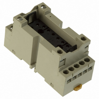
P7S-14F
Manufacturer Part Number
P7S-14F
Description
Contact OSTI
Manufacturer
Omron
Series
G7Sr
Type
Socketr
Specifications of P7S-14F
Number Of Positions
14
Mounting Type
DIN Rail
Termination Style
Screw Terminal
Socket Mounting
DIN Rail
Socket Terminals
Screw
Voltage Rating
24VDC
Rohs Compliant
Yes
Lead Free Status / RoHS Status
Lead free / RoHS Compliant
For Use With/related Products
G7S Series
For Use With
Z2362 - RELAY SAFETY 6A 24VDC PLUG-INZ2363 - RELAY SAFETY 6A 24VDC PLUG-IN
Lead Free Status / RoHS Status
Lead free / RoHS Compliant
Other names
P7S14F
Z2417
Z2417
Available stocks
Company
Part Number
Manufacturer
Quantity
Price
Company:

Part Number:
P7S-14F
Manufacturer:
Omron Electronics Inc-EMC Div
Quantity:
135


B Noise from Contacts
Noise may be transmitted to the electronic circuit when switching a
load, such as a motor or transistor, that generates a surge at the
contacts. When designing patterns, take the following three points
into consideration.
1. Do not place a signal transmission pattern near the contact
2. Shorten the length of patterns that may be sources of noise.
3. Block noise from electronic circuits by means such as
C High-frequency Patterns
As the manipulated frequency is increased, pattern mutual
interference also increases. Therefore, take noise countermeasures
into consideration when designing high-frequency pattern and land
shapes.
G-6 Shape of Lands
1. The land section should be on the center line of the copper-foil
2. A break in the circular land area will prevent molten solder from
G-7 Pattern Conductor Width and Thickness
The following thicknesses of copper foil are standard: 35 μm and
70 μm. The conductor width is determined by the current flow and
allowable temperature rise. Refer to the chart below as a simple
guideline.
Conductor Width and Permissible Current
(According to IEC Pub326-3)
Correct Examples
Incorrect
Examples
pattern.
constructing ground patterns.
pattern, so that the soldered fillets become uniform.
filling holes reserved for components which must be soldered
manually after the automatic soldering of the PCB is complete.
0.5
50
30
20
10
7
5
3
2
7
5
3
2
1
http://www.ia.omron.com/
Cross-sectional area (mm
0.03 0.05 0.07 0.1
0.2 to 0.5 mm
305 /m
35 μm
2
)
Break in land
0.3
610 /m
70 μm
2
0.5 0.7 1
100˚C
75˚C
50˚C
40˚C
30˚C
20˚C
10˚C
2
G-8 Conductor Pitch
The conductor pitch on a PCB is determined by the insulation
characteristics between conductors and the environmental
conditions under which the PCB is to be used. Refer to the following
graph. If the PCB must conform to safety organization standards
(such as UL, CSA, or IEC), however, priority must be given to
fulfilling their requirements. Also, multi-layer PCBs can be used as a
means of increasing the conductor pitch.
Voltage between Conductors vs. Conductor Pitch
(According to IEC Pub326-3)
G-9 Securing the PCB
Although the PCB itself is not normally a source of vibration or shock,
it may prolong vibration or shock by resonating with external vibration
or shock. Securely fix the PCB, paying attention to the following
points.
Rack mounting
Screw mounting
Mounting method
(c)Copyright OMRON Corporation 2007 All Rights Reserved.
3,000
2,000
1,000
700
500
300
200
100
A = Without coating at altitude of 3,000 m max.
B = Without coating at altitude of 3,000 m or higher but lower than 15,000 m
C = With coating at altitude of 3,000 m max.
D = With coating at altitude of 3,000 m or higher
70
50
30
20
0.1
0.2 0.3 0.5 0.7 1.0
No gap between rack's guide and PCB
• Securely tighten screw.
• Attach rubber washers to screws when
Place heavy components such as Relays on
part of PCB near where screws are to be
used.
mounting components that are affected by
shock (such as audio devices.)
2
Conductor pitch (mm)
3
5
Process
10
D
C
A
B
C-12
Related parts for P7S-14F
Image
Part Number
Description
Manufacturer
Datasheet
Request
R

Part Number:
Description:
SOCKET PC MNT FOR G7S RELAY
Manufacturer:
Omron
Datasheet:

Part Number:
Description:
Relay Sockets & Hardware G7 RELAY TRACK MT SOCKET
Manufacturer:
Omron
Datasheet:

Part Number:
Description:
Relay Sockets & Hardware G7 relay PCB mounting
Manufacturer:
Omron
Part Number:
Description:
Relay Sockets & Hardware SOCKET
Manufacturer:
Omron
Datasheet:

Part Number:
Description:
G6S-2GLow Signal Relay
Manufacturer:
Omron Corporation
Datasheet:
Part Number:
Description:
Compact, Low-cost, SSR Switching 5 to 20 A
Manufacturer:
Omron Corporation
Datasheet:
Part Number:
Description:
Manufacturer:
Omron Corporation
Datasheet:
Part Number:
Description:
Manufacturer:
Omron Corporation
Datasheet:
Part Number:
Description:
Manufacturer:
Omron Corporation
Datasheet:
Part Number:
Description:
Manufacturer:
Omron Corporation
Datasheet: