PMEG3015EV,115 NXP Semiconductors, PMEG3015EV,115 Datasheet
PMEG3015EV,115
Specifications of PMEG3015EV,115
PMEG3015EV T/R
PMEG3015EV T/R


Related parts for PMEG3015EV,115


PMEG3015EV,115 Summary of contents
Page 1
PMEG3015EV 30 V, 1.5 A ultra low V SOT666 package Rev. 02 — 4 February 2010 1. Product profile 1.1 General description Planar Maximum Efficiency General Application (MEGA) Schottky barrier rectifier with an integrated guard ring for stress protection, encapsulated ...
Page 2
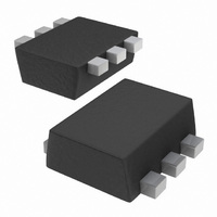
... NXP Semiconductors 2. Pinning information Table 2. Pin Ordering information Table 3. Type number PMEG3015EV 4. Marking Table 4. Type number PMEG3015EV PMEG3015EV_2 Product data sheet 30 V, 1.5 A ultra low V Pinning Description cathode cathode anode anode cathode cathode Ordering information Package Name Description - plastic surface mounted package; 6 leads Marking codes Rev. 02 — ...
Page 3
... NXP Semiconductors 5. Limiting values Table 5. In accordance with the Absolute Maximum Rating System (IEC 60134). Symbol Parameter FRM I FSM P tot amb T stg [1] For SOT666 only valid, if pins 3 and 4 are connected in parallel. [2] Device mounted on an FR4 Printed-Circuit Board (PCB), single-sided copper, tin-plated and standard footprint ...
Page 4
... NXP Semiconductors 7. Characteristics Table amb Symbol [1] Pulse test: t PMEG3015EV_2 Product data sheet 30 V, 1.5 A ultra low V Characteristics ° C unless otherwise specified. Parameter Conditions forward voltage 100 500 1 reverse current diode capacitance MHz R ≤ 300 μs; δ ≤ 0.02. p Rev. 02 — 4 February 2010 ...
Page 5
... NXP Semiconductors (mA (5) 10 (4) (3) (2) ( − 0.2 = −40 °C (1) T amb = 25 °C (2) T amb = 85 °C (3) T amb = 125 °C (4) T amb = 150 °C (5) T amb Fig 1. Forward current as a function of forward voltage; typical values = 25 ° MHz T amb Fig 3. Diode capacitance as a function of reverse voltage; typical values ...
Page 6
... NXP Semiconductors 8. Package outline Fig 4. 9. Packing information Table 8. Packing methods The indicated -xxx are the last three digits of the 12NC ordering code. Type number Package PMEG3015EV SOT666 [1] For further information and the availability of packing methods, see PMEG3015EV_2 Product data sheet ...
Page 7
... NXP Semiconductors 10. Soldering Fig 5. PMEG3015EV_2 Product data sheet 30 V, 1.5 A ultra low V OI1 = 2.750 2.450 2.100 Obl = Pbl = 1.600 1.200 2.200 CU La1 = 2.500 CU Reflow soldering is the only recommended soldering method. Dimensions in mm Reflow soldering footprint SOT666 Rev. 02 — 4 February 2010 PMEG3015EV ...
Page 8
... Revision history Document ID Release date PMEG3015EV_2 20100204 • Modifications: This data sheet was changed to reflect the new company name NXP Semiconductors, including new legal definitions and disclaimers. No changes were made to the technical content. PMEG3015EV_1 20050404 PMEG3015EV_2 Product data sheet 30 V, 1.5 A ultra low V ...
Page 9
... Right to make changes — NXP Semiconductors reserves the right to make changes to information published in this document, including without limitation specifications and product descriptions, at any time and without notice ...
Page 10
... NXP Semiconductors 14. Contents 1 Product profile . . . . . . . . . . . . . . . . . . . . . . . . . . 1 1.1 General description . . . . . . . . . . . . . . . . . . . . . 1 1.2 Features . . . . . . . . . . . . . . . . . . . . . . . . . . . . . . 1 1.3 Applications . . . . . . . . . . . . . . . . . . . . . . . . . . . 1 1.4 Quick reference data . . . . . . . . . . . . . . . . . . . . 1 2 Pinning information . . . . . . . . . . . . . . . . . . . . . . 2 3 Ordering information . . . . . . . . . . . . . . . . . . . . . 2 4 Marking . . . . . . . . . . . . . . . . . . . . . . . . . . . . . . . . 2 5 Limiting values Thermal characteristics . . . . . . . . . . . . . . . . . . 3 7 Characteristics . . . . . . . . . . . . . . . . . . . . . . . . . . 4 8 Package outline . . . . . . . . . . . . . . . . . . . . . . . . . 6 9 Packing information . . . . . . . . . . . . . . . . . . . . . 6 10 Soldering . . . . . . . . . . . . . . . . . . . . . . . . . . . . . . 7 11 Revision history . . . . . . . . . . . . . . . . . . . . . . . . . 8 12 Legal information ...