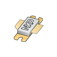
BLF6G20-110 NXP Semiconductors, BLF6G20-110 Datasheet - Page 3

BLF6G20-110
Manufacturer Part Number
BLF6G20-110
Description
RF MOSFET Small Signal LDMOS TNS
Manufacturer
NXP Semiconductors
Datasheet
1.BLF6G20-110.pdf
(10 pages)
Specifications of BLF6G20-110
Configuration
Single
Transistor Polarity
N-Channel
Resistance Drain-source Rds (on)
0.16 Ohms
Drain-source Breakdown Voltage
65 V
Gate-source Breakdown Voltage
13 V
Continuous Drain Current
29 A
Maximum Operating Temperature
+ 225 C
Mounting Style
SMD/SMT
Minimum Operating Temperature
- 65 C
Package / Case
SOT502B
Lead Free Status / RoHS Status
Lead free / RoHS Compliant
Other names
BLF6G20-110,112
Available stocks
Company
Part Number
Manufacturer
Quantity
Price
Company:
Part Number:
BLF6G20-110
Manufacturer:
NXP
Quantity:
1 000
Company:
Part Number:
BLF6G20-110
Manufacturer:
Humirel
Quantity:
5 000
Company:
Part Number:
BLF6G20-110,112
Manufacturer:
ZCOMM
Quantity:
1 400
NXP Semiconductors
5. Thermal characteristics
6. Characteristics
7. Application information
BLF6G20-110_BLF6G20LS-110_3
Product data sheet
7.1 Ruggedness in class-AB operation
Table 5.
Table 6.
T
Table 7.
Mode of operation: 2-carrier W-CDMA; PAR 7 dB at 0.01 % probability on CCDF; 3GPP test
model 1; 1-64 PDPCH; f
RF performance at V
class-AB production test circuit.
The BLF6G20-110 and BLF6G20LS-110 are capable of withstanding a load mismatch
corresponding to VSWR = 10 : 1 through all phases under the following conditions:
V
Symbol
R
Symbol Parameter
V
V
V
I
I
I
g
R
C
Symbol
P
G
IMD3
ACPR
DSS
DSX
GSS
j
fs
DS
D
(BR)DSS
GS(th)
GSq
L(AV)
th(j-case)
DS(on)
rs
p
= 25 C unless otherwise specified.
= 28 V; I
drain-source breakdown
voltage
gate-source threshold voltage
gate-source quiescent voltage V
drain leakage current
drain cut-off current
gate leakage current
forward transconductance
drain-source on-state
resistance
feedback capacitance
Parameter
average output power
power gain
drain efficiency
third order intermodulation distortion
adjacent channel power ratio
Thermal characteristics
Characteristics
Application information
Parameter
thermal resistance from
junction to case
Dq
= 900 mA; P
DS
= 28 V; I
1
Rev. 03 — 13 January 2009
BLF6G20-110; BLF6G20LS-110
= 1932.5 MHz; f
L
Dq
= 110 W (CW); f = 1990 MHz.
= 900 mA; T
Conditions
T
P
case
L
2
Conditions
V
V
V
V
V
V
V
V
I
V
f = 1 MHz
= 25 W (CW)
= 1942.5 MHz; f
D
GS
DS
DS
GS
GS
DS
GS
DS
GS
GS
= 5.25 A
= 80 C;
case
= 10 V; I
= 28 V; I
= 10 V
= 10 V; I
= 0 V; I
= 0 V; V
= V
= 13 V; V
= V
= 0 V; V
GS(th)
GS(th)
= 25 C; unless otherwise specified; in a
Conditions
P
P
P
P
L(AV)
L(AV)
L(AV)
L(AV)
D
DS
DS
D
D
D
= 0.5 mA
+ 3.75 V;
+ 3.75 V;
DS
= 150 mA
= 950 mA
= 7.5 A
= 25 W
= 25 W
= 25 W
= 25 W
Type
BLF6G20-110
BLF6G20LS-110
= 28 V
= 28 V;
3
= 0 V
= 1977.5 MHz; f
Power LDMOS transistor
Min
65
1.4
1.6
-
22.3
-
-
-
-
Min
-
18
28
-
-
4
Typ
-
2
2.1
-
27
-
10.5
0.1
2.1
© NXP B.V. 2009. All rights reserved.
= 1987.5 MHz;
Typ
25
19
32
34
38
Typ
0.52
0.45
Max
-
2.4
2.6
5
-
450
-
0.160
-
Max
-
-
-
28
33
Unit
K/W
K/W
3 of 10
Unit
W
dB
%
dBc
dBc
Unit
V
V
V
A
nA
S
pF
A


