KAC-9618 Eastman Kodak Company, KAC-9618 Datasheet - Page 22
KAC-9618
Manufacturer Part Number
KAC-9618
Description
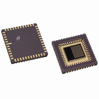
IC SENSOR IMAGE VGA MONO 48-CLCC
Manufacturer
Eastman Kodak Company
Type
CMOS Imagingr
Datasheet
1.KAC-9618.pdf
(43 pages)
Specifications of KAC-9618
Pixel Size
7.5µm x 7.5µm
Active Pixel Array
648H x 488V
Frames Per Second
30
Voltage - Supply
3.3V
Package / Case
48-CLCC
Lead Free Status / RoHS Status
Lead free / RoHS Compliant
Other names
LM9618IEA
LM9618IEA
LM9618IEA
Available stocks
Company
Part Number
Manufacturer
Quantity
Price
Company:

Part Number:
KAC-9618
Manufacturer:
IXYS
Quantity:
2 100


IMAGE SENSOR SOLUTIONS
Functional Description
11.0 DIGITAL VIDEO PORT
The captured image is placed onto a flexible 12-bit digital port as
shown in Figure 10. The digital video port consists of a program-
mable 12-bit digital Data Out Bus (d[11:0]) and three program-
mable synchronisation signals (hsync, vsync, pclk).
By default the synchronisation signals are configured to operate
in “master” mode. They can be programed to operate in “slave”
mode.
The following sections are a detailed description of the timing
and programming modes of digital video port.
Pixel data is output on a 12-bit digital video bus. This bus can be
tri-stated by asserting the TriState bit in the VIDEOMODE1 reg-
ister.
11.1
A programmable matrix switch is provided to map the output of
the internal pixel framer to the pins of the digital video bus as
illustrated in Figure 35.
www.kodak.com/go/imagers 585-722-4385
11
Internal Pixel Framer Output Register
d11
Internal Pixel Framer Output Register
11
11
Internal Pixel Framer Output Register
Digital Video Data Out Bus (d[11:0])
Figure 35. Digital Video Bus Switching Modes
10
11
10
d10
d11 d10 d9 d8 d7 d6 d5 d4 d3 d2 d1
10
d11 d10 d9 d8 d7 d6 d5 d4 d3 d2 d1
9
10
d11 d10 d9 d8 d7 d6 d5 d4 d3 d2 d1 d0
a) MSB Bit 11, Switch Mode (default)
9
Internal Pixel Framer Output Register
d9
9
8
9
b) MSB Bit 10, Switch Mode
8
c) MSB bit 9, Switch Mode
d8
8
7
d) MSB bit 8, Switch Mode
8
7
d7
7
6
7
6
5
d6
6
6
5
4
d5
5
5
4
3
(continued)
4
d4
4
3
2
3
d3
3
2
1
2
d2
1
2
0
1
0
d1 d0
1
0
d0
0
d0
22
This feature allows a programmable digital gain to be imple-
mented when connecting the sensor to 8 or 10 bit digital video
processing systems as illustrated in Figure 36. The unused bits
on the digital video bus can be optionally tri-stated.
a) KAC-9618 Connected to a 10 bit Digital Image Processors
Synchronisation Signals in Master Mode
By default the sensor’s digital video port’s synchronisation sig-
nals are configured to operate in master mode. In master mode
the integrated timing and control block controls the flow of data
onto the 12-bit digital port, three synchronisation outputs are
provided:
11.2
The pixel clock output pin, pclk, is provided to act as a synchro-
nisation reference for the pixel data appearing at the digital
video out bus pins d[11:0]. This pin can be programmed to oper-
ate in two modes:
• In free running mode the pixel clock output pin, pclk, is always
• In data ready mode, the pixel clock output pin (pclk) will pro-
b) KAC-9618 Connected to a 8 bit Digital Image Processors
running with a fixed period. Pixel data appearing on the digital
video bus d[11:0] are synchronized to a specified active edge
of the clock as shown in Figure 37.
duce a pulse with a specified level every time valid pixel data
appears on the digital video bus d[11:0] as shown in Figure
38.
Figure 36. Example of connection to 10/8 bit systems
invalid pixel data
pclk
hsync
vsync
Pixel Clock Output Pin (pclk) (Master Mode)
KAC-
KAC-
Figure 37. pclk in Free Running Mode
pclk
d[11:0]
pclk
d[11:0]
b) pclk active edge positive (default)
is the pixel clock output pin.
is the horizontal synchronisation output signal.
is the vertical synchronisation output signal.
a) pclk active edge negative
d10
d10
d11
d11
d9
d8
d7
d6
d5
d4
d3
d2
d1
d0
d9
d8
d7
d6
d5
d4
d3
d2
d1
d0
Email:imagers@kodak.com
d9
d8
d7
d6
d5
d4
d3
d2
d1
d0
d7
d6
d5
d4
d3
d2
d1
d0
Processor
Processor
Digital
Image
Digital
Image
10 bit
8 bit
Related parts for KAC-9618
Image
Part Number
Description
Manufacturer
Datasheet
Request
R

Part Number:
Description:
IC PROCESSOR IMAGE DGTL REALTIME
Manufacturer:
Eastman Kodak Company

Part Number:
Description:
HEADBOARD FOR KAC-9618
Manufacturer:
Eastman Kodak Company

Part Number:
Description:
HEADBOARD FOR KAC-9619
Manufacturer:
Eastman Kodak Company

Part Number:
Description:
HEADBOARD FOR KAC-9628
Manufacturer:
Eastman Kodak Company

Part Number:
Description:
HEADBOARD FOR KAC-9630
Manufacturer:
Eastman Kodak Company

Part Number:
Description:
HEADBOARD FOR KAC-9637
Manufacturer:
Eastman Kodak Company

Part Number:
Description:
HEADBOARD FOR KAC-9638
Manufacturer:
Eastman Kodak Company

Part Number:
Description:
HEADBOARD FOR KAC-9647
Manufacturer:
Eastman Kodak Company

Part Number:
Description:
HEADBOARD FOR KAC-9648
Manufacturer:
Eastman Kodak Company
Part Number:
Description:
HEADBOARD FOR KAC-9627
Manufacturer:
Eastman Kodak Company
Part Number:
Description:
KIT EVALUATION SENSOR KAC-9618
Manufacturer:
Eastman Kodak Company
Part Number:
Description:
KIT EVALUATION SENSOR KAC-9638
Manufacturer:
Eastman Kodak Company
Part Number:
Description:
KIT EVALUATION SENSOR KAC-9628
Manufacturer:
Eastman Kodak Company
Part Number:
Description:
KIT EVALUATION SENSOR KAC-9637
Manufacturer:
Eastman Kodak Company
Part Number:
Description:
KIT EVALUATION SENSOR KAC-9647
Manufacturer:
Eastman Kodak Company