MT9M001C12STM Aptina LLC, MT9M001C12STM Datasheet - Page 6
MT9M001C12STM
Manufacturer Part Number
MT9M001C12STM
Description
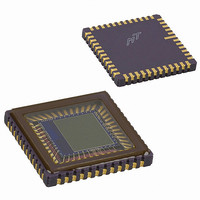
SENSOR IMAGE MONO CMOS 48-LCC
Manufacturer
Aptina LLC
Type
CMOS Imagingr
Datasheets
1.MT9M001C12STM.pdf
(35 pages)
2.MT9M001C12STM.pdf
(2 pages)
3.MT9M001C12STM.pdf
(28 pages)
Specifications of MT9M001C12STM
Pixel Size
5.2µm x 5.2µm
Active Pixel Array
1280H x 1024V
Frames Per Second
30
Voltage - Supply
3 V ~ 3.6 V
Package / Case
48-CLCC
Sensor Image Color Type
Monochrome
Sensor Image Size
1280x1024Pixels
Operating Supply Voltage (min)
3V
Operating Supply Voltage (typ)
3.3V
Operating Supply Voltage (max)
3.6V
Operating Temp Range
0C to 70C
Package Type
CLCC
Operating Temperature Classification
Commercial
Mounting
Surface Mount
Pin Count
48
Lead Free Status / RoHS Status
Lead free / RoHS Compliant
Other names
557-1151
Q3930625
Q3990821
Q3930625
Q3990821
Available stocks
Company
Part Number
Manufacturer
Quantity
Price
Company:

Part Number:
MT9M001C12STM
Manufacturer:
MICRON
Quantity:
1 000
Part Number:
MT9M001C12STM
Manufacturer:
MICRON/镁光
Quantity:
20 000


Table 3:
PDF: 09005aef81c2856f/Source: 09005aef80a3e031
MT9M001_DS_2.fm - Rev. F 5/06 EN
15,17,18,21, 47,
Pin Numbers
12,14, 19, 30,
24–28, 32–36
2, 3 ,6, 9, 11,
5, 23, 38, 43
4, 22, 37
16, 20
42, 44
29
13
10
46
45
41
40
31
39
48
7
8
1
Pin Descriptions
FRAME_VALID
LINE_VALID
D
STANDBY
TRIGGER
Symbol
OUT
STROBE
VAAPIX
RESET#
PIXCLK
CLKIN
S
A
D
SCLK
OE#
V
V
DATA
NC
GND
GND
<0–9>
AA
DD
Input/Output
Output
Output
Output
Output
Output
Supply
Supply
Supply
Supply
Supply
Input
Input
Input
Input
Input
Input
Type
—
MT9M001: 1/2-Inch Megapixel Digital Image Sensor
Clock in. Master clock into sensor (48 MHz maximum).
Output enable. OE# when HIGH places outputs D
FRAME_VALID, LINE_VALID, PIXCLK, and STROBE into a tri-state
configuration.
Reset. Activates (LOW) asynchronous reset of sensor. All registers
assume factory defaults.
Serial clock. Clock for serial interface.
Standby. Activates (HIGH) standby mode, disables analog bias circuitry
for power saving mode.
Trigger. Activates (HIGH) snapshot sequence.
Serial data. Serial data bus, requires 1.5
Data out. Pixel data output bits 0:9, D
Frame valid. Output is pulsed HIGH during frame of valid pixel data.
Line valid. Output is pulsed HIGH during line of selectable valid pixel
data (see Reg0x20 for options).
Pixel clock. Pixel data outputs are valid during falling edge of this
clock. Frequency = (master clock).
Strobe. Output is pulsed HIGH to indicate sensor reset operation of
pixel array has completed.
Analog ground. Provide isolated ground for analog block and pixel
array.
Digital ground. Provide isolated ground for digital block.
Analog power. Provide power supply for analog block, 3.3V ±0.3V.
Analog pixel power. Provide power supply for pixel array, 3.3V ±0.3V
(3.3V).
Digital power. Provide power supply for digital block, 3.3V ±0.3V.
No connect. These pins must be left unconnected.
6
Micron Technology, Inc., reserves the right to change products or specifications without notice.
Description
OUT
KΩ
<9> (MSB), D
General Description
resistor to 3.3V for pull-up.
©2004 Micron Technology, Inc. All rights reserved.
OUT
<0:9>,
OUT
<0> (LSB).
Related parts for MT9M001C12STM
Image
Part Number
Description
Manufacturer
Datasheet
Request
R

Part Number:
Description:
SENSOR IMAGE VGA COLOR CMOS PLCC
Manufacturer:
Aptina LLC
Datasheet:

Part Number:
Description:
IC SENSOR IMAGE COLOR 48CLCC
Manufacturer:
Aptina LLC
Datasheet:

Part Number:
Description:
SENSOR IMAGE 1.3MP CMOS 48-CLCC
Manufacturer:
Aptina LLC
Datasheet:

Part Number:
Description:
SENSOR IMAGE 2MP CMOS 48-CLCC
Manufacturer:
Aptina LLC
Datasheet:

Part Number:
Description:
SENSOR IMAGE VGA MONO 52IBGA
Manufacturer:
Aptina LLC
Datasheet:

Part Number:
Description:
SENSOR IMAGE VGA COLOR 48CLCC
Manufacturer:
Aptina LLC
Datasheet:

Part Number:
Description:
SENSOR IMAGE COLOR CMOS 48-PLCC
Manufacturer:
Aptina LLC
Datasheet:

Part Number:
Description:
KIT HEAD BOARD FOR MT9P031
Manufacturer:
Aptina LLC
Datasheet:

Part Number:
Description:
KIT HEAD BOARD FOR MT9D131
Manufacturer:
Aptina LLC
Datasheet:

Part Number:
Description:
KIT HEAD BOARD FOR MT9P031
Manufacturer:
Aptina LLC
Datasheet:
Part Number:
Description:
SENSOR IMAGE VGA COLOR CMOS PLCC
Manufacturer:
Aptina LLC
Datasheet:
Part Number:
Description:
IC SENSOR IMAGE COLOR 48CLCC
Manufacturer:
Aptina LLC
Datasheet:
Part Number:
Description:
SENSOR IMAGE 2MP CMOS 48-CLCC
Manufacturer:
Aptina LLC
Datasheet:
