MT9M001C12STM Aptina LLC, MT9M001C12STM Datasheet - Page 18
MT9M001C12STM
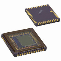
Manufacturer Part Number
MT9M001C12STM
Description
SENSOR IMAGE MONO CMOS 48-LCC
Manufacturer
Aptina LLC
Type
CMOS Imagingr
Datasheets
1.MT9M001C12STM.pdf
(35 pages)
2.MT9M001C12STM.pdf
(2 pages)
3.MT9M001C12STM.pdf
(28 pages)
Specifications of MT9M001C12STM
Pixel Size
5.2µm x 5.2µm
Active Pixel Array
1280H x 1024V
Frames Per Second
30
Voltage - Supply
3 V ~ 3.6 V
Package / Case
48-CLCC
Sensor Image Color Type
Monochrome
Sensor Image Size
1280x1024Pixels
Operating Supply Voltage (min)
3V
Operating Supply Voltage (typ)
3.3V
Operating Supply Voltage (max)
3.6V
Operating Temp Range
0C to 70C
Package Type
CLCC
Operating Temperature Classification
Commercial
Mounting
Surface Mount
Pin Count
48
Lead Free Status / RoHS Status
Lead free / RoHS Compliant
Other names
557-1151
Q3930625
Q3990821
Q3930625
Q3990821
Available stocks
Company
Part Number
Manufacturer
Quantity
Price
Company:

Part Number:
MT9M001C12STM
Manufacturer:
MICRON
Quantity:
1 000
Part Number:
MT9M001C12STM
Manufacturer:
MICRON/镁光
Quantity:
20 000


Table 7:
PDF: 09005aef81c2856f/Source: 09005aef80a3e031
MT9M001_DS_2.fm - Rev. F 5/06 EN
Register
Test Data
Read Mode 2
This register is used to control many aspects of the readout of the sensor.
Test Data
Black Level Calibration
These registers are used in the black level calibration. Their functionality is described in detail in the next section.
0x2D
0x2E
0x35
0x32
0x20
0x32
Register Description (continued)
11:2
11:2
Bit
6:0
6:0
6:0
10
11
12
13
14
15
0
1
2
3
4
5
6
7
8
9
Even row, odd column
Odd row, odd column
Global gain
Test Data.
The value used to produce a test pattern in “Use Test Data” mode (Reg0x07 bit 6).
No bad frames
0 (default) = only output good frames. A bad frame is defined as the first frame following a change
to: window size or position, horizontal blanking, row or column skip, or mirroring.
Reserved
Reserved
Column skip
col 5…).
0 = normal readout (default).
Row skip
5…).
0 = normal readout (default).
Reserved
Reserved
Flip Row
0 (default) = normal readout.
Reserved
1 = "Continuous" LINE_VALID (continue producing LINE_VALID during vertical blanking).
0 = normal LINE_VALID (default, no LINE_VALID during vertical blanking).
1 = LINE_VALID = "Continuous" LINE_VALID XOR FRAME_VALID.
0 = LINE_VALID determined by bit 9.
Reserved
Reserved
Reserved
Reserved
Mirror Row
0 (default) = normal readout (top to bottom).
Test Data.
The value used to produce a test pattern in “Use Test Data” mode (Reg0x07 bit 6).
—
—
—
—
—
—
—
—
—
—
—
1 = readout starting 1 row later (alternate color pair).
default is 0; do not change.
default is 1; set to “1” at all times.
1 = read out two rows, and then skip two rows (for example, row 0, row 1, row 4, row
default is 0; do not change.
default is 0; set to zero at all times.
default is 1; set to “1” at all times.
default is 0; do not change.
default is 1; do not change.
default is 0; do not change.
default is 0; do not change.
—
—
—
1 = read out from bottom to top (upside down).
default = 0x08 (8) = 1x gain. This register can be used to set all four gains at once.
—
1= read out two columns, and then skip two columns (for example, col 0, col 1, col 4,
1 = output all frames (including bad frames).
—
—
default = 0x08 (8) = 1x gain.
default = 0x08 (8) = 1x gain.
MT9M001: 1/2-Inch Megapixel Digital Image Sensor
18
Description
Micron Technology, Inc., reserves the right to change products or specifications without notice.
©2004 Micron Technology, Inc. All rights reserved.
Registers
Related parts for MT9M001C12STM
Image
Part Number
Description
Manufacturer
Datasheet
Request
R

Part Number:
Description:
SENSOR IMAGE VGA COLOR CMOS PLCC
Manufacturer:
Aptina LLC
Datasheet:

Part Number:
Description:
IC SENSOR IMAGE COLOR 48CLCC
Manufacturer:
Aptina LLC
Datasheet:

Part Number:
Description:
SENSOR IMAGE 1.3MP CMOS 48-CLCC
Manufacturer:
Aptina LLC
Datasheet:

Part Number:
Description:
SENSOR IMAGE 2MP CMOS 48-CLCC
Manufacturer:
Aptina LLC
Datasheet:

Part Number:
Description:
SENSOR IMAGE VGA MONO 52IBGA
Manufacturer:
Aptina LLC
Datasheet:

Part Number:
Description:
SENSOR IMAGE VGA COLOR 48CLCC
Manufacturer:
Aptina LLC
Datasheet:

Part Number:
Description:
SENSOR IMAGE COLOR CMOS 48-PLCC
Manufacturer:
Aptina LLC
Datasheet:

Part Number:
Description:
KIT HEAD BOARD FOR MT9P031
Manufacturer:
Aptina LLC
Datasheet:

Part Number:
Description:
KIT HEAD BOARD FOR MT9D131
Manufacturer:
Aptina LLC
Datasheet:

Part Number:
Description:
KIT HEAD BOARD FOR MT9P031
Manufacturer:
Aptina LLC
Datasheet:
Part Number:
Description:
SENSOR IMAGE VGA COLOR CMOS PLCC
Manufacturer:
Aptina LLC
Datasheet:
Part Number:
Description:
IC SENSOR IMAGE COLOR 48CLCC
Manufacturer:
Aptina LLC
Datasheet:
Part Number:
Description:
SENSOR IMAGE 2MP CMOS 48-CLCC
Manufacturer:
Aptina LLC
Datasheet:
