MT9M001C12STM Aptina LLC, MT9M001C12STM Datasheet - Page 21
MT9M001C12STM
Manufacturer Part Number
MT9M001C12STM
Description
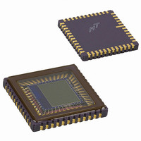
SENSOR IMAGE MONO CMOS 48-LCC
Manufacturer
Aptina LLC
Type
CMOS Imagingr
Datasheets
1.MT9M001C12STM.pdf
(35 pages)
2.MT9M001C12STM.pdf
(2 pages)
3.MT9M001C12STM.pdf
(28 pages)
Specifications of MT9M001C12STM
Pixel Size
5.2µm x 5.2µm
Active Pixel Array
1280H x 1024V
Frames Per Second
30
Voltage - Supply
3 V ~ 3.6 V
Package / Case
48-CLCC
Sensor Image Color Type
Monochrome
Sensor Image Size
1280x1024Pixels
Operating Supply Voltage (min)
3V
Operating Supply Voltage (typ)
3.3V
Operating Supply Voltage (max)
3.6V
Operating Temp Range
0C to 70C
Package Type
CLCC
Operating Temperature Classification
Commercial
Mounting
Surface Mount
Pin Count
48
Lead Free Status / RoHS Status
Lead free / RoHS Compliant
Other names
557-1151
Q3930625
Q3990821
Q3930625
Q3990821
Available stocks
Company
Part Number
Manufacturer
Quantity
Price
Company:

Part Number:
MT9M001C12STM
Manufacturer:
MICRON
Quantity:
1 000
Part Number:
MT9M001C12STM
Manufacturer:
MICRON/镁光
Quantity:
20 000


Feature Description
Signal Path
Programmable Gain Stage
Figure 10: Signal Path
Table 8:
PDF: 09005aef81c2856f/Source: 09005aef80a3e031
MT9M001_DS_2.fm - Rev. F 5/06 EN
Nominal Gain
4.25 to 8.00
1 to 4.000
Recommended Gain Settings at 48 MHz
9 to 15
The MT9M001 signal path consists of two stages, a programmable gain stage and a
programmable analog offset stage.
A total programmable gain of 15 is available and can be calculated using the following
formula:
For gain higher than eight, the user would need to set bit[6:5] = 11 and use the lower 3
LSB's bit[2:0] to set the higher gain values. The formula for obtaining gain greater than
eight is as follows:
For example, for total gain = 12, the value to program is bit[6–0] = 1100100.
The maximum total gain = 15, i.e. bit[6:0] = 1100111.
The gain circuitry in the MT9M001 is designed to offer signal gains from one to 15. The
minimum gain of one corresponds to the lowest setting where the pixel signal is guaran-
teed to saturate the ADC under all specified operating conditions. Any reduction of the
gain below this value may cause the sensor to saturate at ADC output values less than
the maximum, under certain conditions. It is recommended that this guideline be
followed at all times.
Since bit[6] of the gain registers are multiplicative factors for the gain settings, there are
alternative ways of achieving certain gains. Some settings offer superior noise perfor-
mance to others, despite the same overall gain. Recommended gain settings are listed in
Table 8.
Pixel Output
minus reset)
Gain 1 to 8: Gain = (bit[6] + 1) x (bit[5:0] x 0.125)
Total gain = 8 + bit[2:0]
(signal
(Reg0x2B - 0x2E)
Gain Selection
Increments
X
(signed lower 9 bits) x 2mV
Offset Correction Voltage
(Reg0x60, Reg0x61,
0.125
Reg0x63, Reg0x64)
0.25
1.0
MT9M001: 1/2-Inch Megapixel Digital Image Sensor
+
21
10-bit ADC
Recommended Settings
Micron Technology, Inc., reserves the right to change products or specifications without notice.
0x08 to 0x20
0x51 to 0x60
0x61 to 0x67
ADC Data
(9:0)
©2004 Micron Technology, Inc. All rights reserved.
Feature Description
Related parts for MT9M001C12STM
Image
Part Number
Description
Manufacturer
Datasheet
Request
R

Part Number:
Description:
SENSOR IMAGE VGA COLOR CMOS PLCC
Manufacturer:
Aptina LLC
Datasheet:

Part Number:
Description:
IC SENSOR IMAGE COLOR 48CLCC
Manufacturer:
Aptina LLC
Datasheet:

Part Number:
Description:
SENSOR IMAGE 1.3MP CMOS 48-CLCC
Manufacturer:
Aptina LLC
Datasheet:

Part Number:
Description:
SENSOR IMAGE 2MP CMOS 48-CLCC
Manufacturer:
Aptina LLC
Datasheet:

Part Number:
Description:
SENSOR IMAGE VGA MONO 52IBGA
Manufacturer:
Aptina LLC
Datasheet:

Part Number:
Description:
SENSOR IMAGE VGA COLOR 48CLCC
Manufacturer:
Aptina LLC
Datasheet:

Part Number:
Description:
SENSOR IMAGE COLOR CMOS 48-PLCC
Manufacturer:
Aptina LLC
Datasheet:

Part Number:
Description:
KIT HEAD BOARD FOR MT9P031
Manufacturer:
Aptina LLC
Datasheet:

Part Number:
Description:
KIT HEAD BOARD FOR MT9D131
Manufacturer:
Aptina LLC
Datasheet:

Part Number:
Description:
KIT HEAD BOARD FOR MT9P031
Manufacturer:
Aptina LLC
Datasheet:
Part Number:
Description:
SENSOR IMAGE VGA COLOR CMOS PLCC
Manufacturer:
Aptina LLC
Datasheet:
Part Number:
Description:
IC SENSOR IMAGE COLOR 48CLCC
Manufacturer:
Aptina LLC
Datasheet:
Part Number:
Description:
SENSOR IMAGE 2MP CMOS 48-CLCC
Manufacturer:
Aptina LLC
Datasheet:
