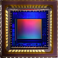
MT9M131C12STC Aptina LLC, MT9M131C12STC Datasheet - Page 4

MT9M131C12STC
Manufacturer Part Number
MT9M131C12STC
Description
SENSOR IMAGE 1.3MP CMOS 48-CLCC
Manufacturer
Aptina LLC
Type
CMOS Imagingr
Series
DigitalClarity®r
Specifications of MT9M131C12STC
Pixel Size
3.6µm x 3.6µm
Active Pixel Array
1280H x 1024V
Frames Per Second
15
Voltage - Supply
2.5 V ~ 3.1 V
Package / Case
48-CLCC
Sensor Image Color Type
Color
Sensor Image Size
1280x1024Pixels
Operating Supply Voltage (min)
2.5V
Operating Supply Voltage (typ)
2.8V
Operating Supply Voltage (max)
3.1V
Operating Temp Range
-30C to 70C
Package Type
CLCC
Operating Temperature Classification
Commercial
Mounting
Surface Mount
Pin Count
48
Lead Free Status / RoHS Status
Lead free / RoHS Compliant
For Use With
557-1251 - KIT HEAD BOARD FOR MT9M131557-1246 - KIT DEV FOR MT9M131
Lead Free Status / RoHS Status
Compliant, Lead free / RoHS Compliant
Other names
557-1312
Available stocks
Company
Part Number
Manufacturer
Quantity
Price
Part Number:
MT9M131C12STC
Manufacturer:
APTTINA
Quantity:
20 000
Functional Overview
Figure 2:
PDF:09005aef824c90f2/Source: 09005aef824c90f9
MT9M131_LDS_2.fm - Rev. A 3/07 EN
V
DD
STANDBY
V
V
Q/D
DD
AA
VAAPIX
CLK_IN
/D
/A
S
GND
SCLK
DATA
OE#
GND
GND
Q
Functional Block Diagram
(Two-Wire Serial I/F Transactions) +
Sensor control (gains, shutter, etc.)
1,316H x 1,048V including black
1/3-inch optical format
Auto black compensation
Programmable analog gain
Programmable exposure
Dual 10-bit ADCs
Low-power preview mode
H/W context switch to/from preview
Bayer RGB output
Image Flow Processor
The MT9M131 is a fully-automatic, single-chip camera, requiring only a power supply,
lens, and clock source for basic operation. Output video is streamed through a parallel
8-bit D
The output pixel clock is used to latch data, while FV and LV signals indicate the active
video. The MT9M131 internal registers are configured using a two-wire serial interface.
The device can be put in low-power sleep mode by asserting STANDBY and shutting
down the clock. Output pins can be tri-stated by de-asserting OE#. Both tri-stating
output pins and entry in standby mode also can be achieved by two-wire serial interface
register writes.
The MT9M131 accepts input clocks up to 54 MHz, delivering up to 15 fps for SXGA reso-
lution images, and up to 30 fps for QSXGA (full field-of-view, sensor pixel skipping)
images. The device also supports a low- power preview configuration that delivers SXGA
images at 7.5 fps and QSXGA images at 30 fps. The device can be programmed to slow
the frame rate in low-light conditions to achieve longer exposures and better image
quality.
Auto exposure
Auto white balance
Flicker detect/avoid
Camera control:
snapshots, flash, video, clip
Camera Control
Control Bus
Sensor Core
OUT
port, shown in Figure 2.
MT9M131: SOC Megapixel Digital Image Sensor
Image Data
Control Bus
(Two-Wire
4
Serial I/F
(Two-Wire Serial I/F
Trans.)
Transactions)
Pixel Data
Control Bus
Micron Technology, Inc., reserves the right to change products or specifications without notice.
Image Flow Processor
Lens shading correction
Color interpolation
Filtered resize and zoom
Defect correction
Color correction
Gamma correction
Color conversion + formatting
Output FIFO
Line Buffers
Colorpipe
SRAM
Functional Overview
©2007 Micron Technology, Inc. All rights reserved.
Preliminary
D
PIXCLK
FV
LV
STROBE
OUT
[7:0]


