MT9M131C12STC Aptina LLC, MT9M131C12STC Datasheet - Page 13
MT9M131C12STC
Manufacturer Part Number
MT9M131C12STC
Description
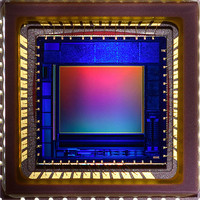
SENSOR IMAGE 1.3MP CMOS 48-CLCC
Manufacturer
Aptina LLC
Type
CMOS Imagingr
Series
DigitalClarity®r
Specifications of MT9M131C12STC
Pixel Size
3.6µm x 3.6µm
Active Pixel Array
1280H x 1024V
Frames Per Second
15
Voltage - Supply
2.5 V ~ 3.1 V
Package / Case
48-CLCC
Sensor Image Color Type
Color
Sensor Image Size
1280x1024Pixels
Operating Supply Voltage (min)
2.5V
Operating Supply Voltage (typ)
2.8V
Operating Supply Voltage (max)
3.1V
Operating Temp Range
-30C to 70C
Package Type
CLCC
Operating Temperature Classification
Commercial
Mounting
Surface Mount
Pin Count
48
Lead Free Status / RoHS Status
Lead free / RoHS Compliant
For Use With
557-1251 - KIT HEAD BOARD FOR MT9M131557-1246 - KIT DEV FOR MT9M131
Lead Free Status / RoHS Status
Compliant, Lead free / RoHS Compliant
Other names
557-1312
Available stocks
Company
Part Number
Manufacturer
Quantity
Price

Part Number:
MT9M131C12STC
Manufacturer:
APTTINA
Quantity:
20 000


Figure 10:
PDF:09005aef824c90f2/Source: 09005aef824c90f9
MT9M131_LDS_2.fm - Rev. A 3/07 EN
Micron, the M logo, the Micron logo, and DigitalClarity are trademarks of Micron Technology, Inc. All other trademarks are
Preliminary: This data sheet contains initial characterization limits that are subject to change upon full characterization of
0.40 ±0.05
Seating
8.8
4X
1.0 ±0.2
plane
48X
47X
4.4
0.2
D
A
48-Pin CLCC Package
over Ni plating, 1.27 microns
Notes:
prodmktg@micron.com www.micron.com Customer Comment Line: 800-932-4992
5.215
Au plating, 0.50 microns
4.4
minimum thickness
minimum thickness
8000 S. Federal Way, P.O. Box 6, Boise, ID 83707-0006, Tel: 208-368-3900
11.43
48
1. Optical center = package center.
2. An IR-cut filter is required to obtain optimal image quality.
3. All dimensions are in millimeters.
8.8
1
Lead finish:
TYP
0.8
5.715
the property of their respective owners.
0.8 TYP
1.7
B
1.75
5.715
4.84
48X R 0.15
5.215
production devices.
for reference only
for reference only
1.400 ±0.125
2.3 ±0.2
11.43
C
MT9M131: SOC Megapixel Digital Image Sensor
13
A
0.90
0.35
0.05
®
Micron Technology, Inc., reserves the right to change products or specifications without notice.
Substrate material: alumina ceramic 0.7 thickness
Wall material: alumina ceramic
Lid material: borosilicate glass 0.55 thickness
Image
sensor die:
0.675 thickness
0.10 A
Ø0.20 A B C
V CTR
Optical
Optical area:
Maximum rotation of optical area relative to package edges: 1º
Maximum tilt of optical area relative to
Maximum tilt of optical area relative to
area
seating plane A : 50 microns
top of cover glass D : 100 microns
Package Dimensions
Ø0.20 A B C
©2007 Micron Technology, Inc. All rights reserved.
10.9 ±0.1
H CTR
CTR
Preliminary
Optical
center
10.9 ±0.1
First
clear
pixel
CTR
1
Related parts for MT9M131C12STC
Image
Part Number
Description
Manufacturer
Datasheet
Request
R

Part Number:
Description:
SENSOR IMAGE VGA COLOR CMOS PLCC
Manufacturer:
Aptina LLC
Datasheet:

Part Number:
Description:
IC SENSOR IMAGE COLOR 48CLCC
Manufacturer:
Aptina LLC
Datasheet:

Part Number:
Description:
SENSOR IMAGE 2MP CMOS 48-CLCC
Manufacturer:
Aptina LLC
Datasheet:

Part Number:
Description:
SENSOR IMAGE VGA MONO 52IBGA
Manufacturer:
Aptina LLC
Datasheet:

Part Number:
Description:
SENSOR IMAGE VGA COLOR 48CLCC
Manufacturer:
Aptina LLC
Datasheet:

Part Number:
Description:
SENSOR IMAGE COLOR CMOS 48-PLCC
Manufacturer:
Aptina LLC
Datasheet:

Part Number:
Description:
KIT HEAD BOARD FOR MT9P031
Manufacturer:
Aptina LLC
Datasheet:

Part Number:
Description:
KIT HEAD BOARD FOR MT9D131
Manufacturer:
Aptina LLC
Datasheet:

Part Number:
Description:
KIT HEAD BOARD FOR MT9P031
Manufacturer:
Aptina LLC
Datasheet:

Part Number:
Description:
KIT HEAD BOARD FOR MT9M032
Manufacturer:
Aptina LLC
Datasheet:
Part Number:
Description:
SENSOR IMAGE VGA COLOR CMOS PLCC
Manufacturer:
Aptina LLC
Datasheet:
Part Number:
Description:
IC SENSOR IMAGE COLOR 48CLCC
Manufacturer:
Aptina LLC
Datasheet:
Part Number:
Description:
SENSOR IMAGE 2MP CMOS 48-CLCC
Manufacturer:
Aptina LLC
Datasheet:
