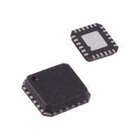
AD8340ACPZ-WP Analog Devices Inc, AD8340ACPZ-WP Datasheet - Page 17

AD8340ACPZ-WP
Manufacturer Part Number
AD8340ACPZ-WP
Description
IC MOD VECT 700-1000MHZ 24-LFCSP
Manufacturer
Analog Devices Inc
Datasheet
1.AD8340ACPZ-REEL7.pdf
(20 pages)
Specifications of AD8340ACPZ-WP
Function
Vector, Modulator
Lo Frequency
700MHz ~ 1GHz
Rf Frequency
700MHz ~ 1GHz
P1db
11dBm
Noise Floor
-149dBm/Hz
Current - Supply
150mA
Voltage - Supply
4.75 V ~ 5.25 V
Test Frequency
880MHz
Package / Case
24-VFQFN, CSP Exposed Pad
Lead Free Status / RoHS Status
Lead free / RoHS Compliant
Table 4. Evaluation Board Configuration Options
Components
R7, R9, R11, R14,
R15, R19, R20, R21,
C15, C19, W3, W4
R1, R3, R10, R12,
R13, R16, R17, R18,
C16, C20, W1, W2
C11, C12
T1, C17, C18, L1, L2
L3, L4, C5, C6
C2, C4, C7, C9, C14,
C1, C3, C8, C10,
R2, R4, R5, R6
R8, SW1
Description
I Channel Baseband Interface. Resistor R7 and Resistor R9 can be
installed to accommodate a baseband source that requires a
specific terminating impedance. C15 and C19 are bypass
capacitors. For single-ended baseband drive, Potentiometer R11
can be used to provide a bias level to the unused input (install
either W3 or W4).
Q Channel Baseband Interface. See the I Channel Baseband
Interface description.
Baseband Low-Pass Filtering. By adding Capacitor C11 between
QFLP and QFLM, and Capacitor C12 between IFLP and IFLM, the
3 dB low-pass corner frequency of the baseband interface can be
reduced from 230 MHz (nominal). See the equation in the
Evaluation Board section.
Output Interface. The 1:1 balun transformer, T1, converts the 50 Ω
differential output to 50 Ω single-ended. C17 and C18 are dc
blocks. L1 and L2 provide dc bias for the output.
Input Interface. The input impedance of the AD8340 requires 5.6 nH
inductors in series with RFIP and RFIM for optimum return loss
when driven by a single-ended 50 Ω line. C5 and C6 are dc blocks.
Supply Decoupling.
Output Disable Interface. The output stage of the AD8340 is
disabled by applying a high voltage to the DSOP pin by moving
SW1 to Position B. The output stage is enabled by moving SW1 to
Position A. The output disable function can also be exercised by
applying an external high or low voltage to the DSOP SMA
connector with SW1 in Position A.
Rev. B | Page 17 of 20
Default Conditions
R7, R9 = open
R11 = potentiometer, 2 kΩ, 10 turns (Bourns)
R14 = 4 kΩ (Size 0603)
R15 = 44 kΩ (Size 0603)
R19, R20, R21 = 0 Ω (Size 0603)
C15, C19 = 0.1 μF (Size 0603)
W3 = jumper (installed)
W4 = jumper (open)
R1, R3 = open
R10 = potentiometer, 2 kΩ, 10 turns (Bourns)
R12 = 4 kΩ (Size 0603)
R13 = 44 kΩ (Size 0603)
R16, R17, R18 = 0 Ω (Size 0603)
C16, C20 = 0.1 μF (Size 0603)
W1 = jumper (installed)
W2 = jumper (open)
C11, C12 = open
C17, C18 = 100 pF (Size 0603)
T1 = ETC1-1-13 (M/A-COM)
L1, L2 = 120 nH (Size 0603)
L3, L4 = 5.6 nH (Size 0402)
C5, C6 = 100 pF (Size 0603)
C2, C4, C7, C9 = open (Size 0603)
C1, C3, C8, C10, C14 = 0.1 μF (Size 0603)
R2, R4, R5, R6 = 0 Ω (Size 0603)
R8 = 10 kΩ (Size 0603)
SW1 = SPDT (Position A, output enabled)
AD8340


