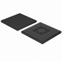
LH7A404N0F092B3;55 NXP Semiconductors, LH7A404N0F092B3;55 Datasheet - Page 47

LH7A404N0F092B3;55
Manufacturer Part Number
LH7A404N0F092B3;55
Description
LH7A404N0F092B3/LFBGA324/TRAYD
Manufacturer
NXP Semiconductors
Series
BlueStreak ; LH7Ar
Datasheet
1.LH7A404N0F000B355.pdf
(75 pages)
Specifications of LH7A404N0F092B3;55
Core Processor
ARM9
Core Size
16/32-Bit
Speed
266MHz
Connectivity
EBI/EMI, IrDA, Microwire, MMC, PS2, SmartCard, SPI, SSI, SSP, UART/USART, USB
Peripherals
AC'97, DMA, LCD, POR, PWM, WDT
Number Of I /o
64
Program Memory Type
ROMless
Ram Size
80K x 8
Voltage - Supply (vcc/vdd)
1.71 V ~ 3.6 V
Data Converters
A/D 9x10b
Oscillator Type
External
Operating Temperature
-40°C ~ 85°C
Package / Case
324-LFBGA
Processor Series
LH7A4
Core
ARM9TDMI
Data Bus Width
32 bit
Mounting Style
SMD/SMT
3rd Party Development Tools
MDK-ARM, RL-ARM, ULINK2
Lead Free Status / RoHS Status
Lead free / RoHS Compliant
For Use With
568-4304 - BOARD EVAL FOR LH7A404
Eeprom Size
-
Program Memory Size
-
Lead Free Status / Rohs Status
Details
Other names
568-4336
935285071557
LH7A404N0F092B3
935285071557
LH7A404N0F092B3
32-Bit System-on-Chip
Synchronous Memory Controller Waveforms
chronous Burst Read (page already open). Figure 19
shows the waveform and timing for synchronous mem-
ory to activate a bank and Write.
Preliminary data sheet
NOTES:
1. SDRAMcmd is the combination of nRAS, nCAS, nSDWE, and nSDCSx.
2. tOVXXX represents tOVRA, tOVCA, tOVSDW, or tOVSC.
3. tOHXXX represents tOHRA, tOHCA, tOHSDW, or tOHSC.
4. nDQM is static LOW.
5. SDCKE is static HIGH.
SDRAMcmd
SBANK[1:0]
Figure 18 shows the waveform and timing for a Syn-
SA[13:0],
D[31:0]
SCLK
SSPTXD/
SSPFRM
SSPRXD
SSPCLK
Figure 19. Synchronous Bank Activate and Write
tOVA
t OVXXX
Figure 18. Synchronous Burst Read
MSB
READ
COLUMN
BANK,
t OHXXX
t OVB
NXP Semiconductors
4 to 16 BITS
tISD tIHD
DATA n
DATA n + 1
LSB
DATA n + 2
DATA n + 3
LH7A404-24
LH7A404
LH7A404-13
47


