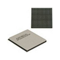
EP2SGX90EF1152I4N Altera, EP2SGX90EF1152I4N Datasheet - Page 12

EP2SGX90EF1152I4N
Manufacturer Part Number
EP2SGX90EF1152I4N
Description
Stratix II GX
Manufacturer
Altera
Datasheet
1.EP2SGX90EF1152I4N.pdf
(316 pages)
Specifications of EP2SGX90EF1152I4N
Family Name
Stratix II GX
Number Of Logic Blocks/elements
90960
# I/os (max)
558
Frequency (max)
732.1MHz
Process Technology
SRAM
Operating Supply Voltage (typ)
1.2V
Logic Cells
90960
Ram Bits
4520448
Operating Supply Voltage (min)
1.15V
Operating Supply Voltage (max)
1.25V
Operating Temp Range
-40C to 100C
Operating Temperature Classification
Industrial
Mounting
Surface Mount
Pin Count
1152
Package Type
FC-FBGA
Lead Free Status / Rohs Status
Compliant
Available stocks
Company
Part Number
Manufacturer
Quantity
Price
Company:
Part Number:
EP2SGX90EF1152I4N
Manufacturer:
ALTERA
Quantity:
535
Part Number:
EP2SGX90EF1152I4N
Manufacturer:
ALTERA/阿尔特拉
Quantity:
20 000
- Current page: 12 of 316
- Download datasheet (2Mb)
Transceivers
2–4
Stratix II GX Device Handbook, Volume 1
capable of built-in self test (BIST) generation and verification. The
ALT2GXB megafunction in the Quartus II software provides a
step-by-step menu selection to configure the transceiver.
Figure 2–1
channel. Stratix II GX transceivers provide PCS and PMA
implementations for all supported protocols. The PCS portion of the
transceiver consists of the word aligner, lane deskew FIFO buffer, rate
matcher FIFO buffer, 8B/10B encoder and decoder, byte serializer and
deserializer, byte ordering, and phase compensation FIFO buffers.
Each Stratix II GX transceiver channel is also capable of BIST generation
and verification in addition to various loopback modes. The PMA portion
of the transceiver consists of the serializer and deserializer, the CRU, and
the high-speed differential transceiver buffers that contain pre-emphasis,
programmable on-chip termination (OCT), programmable voltage
output differential (V
Transmitter Path
This section describes the data path through the Stratix II GX transmitter.
The Stratix II GX transmitter contains the following modules:
■
■
■
■
■
■
■
■
Transmitter PLLs
Each transceiver block has two transmitter PLLs which receive two
reference clocks to generate timing and the following clocks:
■
■
The serializer uses high-speed clocks to transmit data. The serializer is
also referred to as parallel in serial out (PISO). The high-speed clock is fed
to the local clock generation buffer. The local clock generation buffers
divide the high-speed clock on the transmitter to a desired frequency on
a per-channel basis.
clocks.
Transmitter PLLs
Access to one of two PLLs
Transmitter logic array interface
Transmitter phase compensation FIFO buffer
Byte serializer
8B/10B encoder
Serializer (parallel-to-serial converter)
Transmitter differential output buffer
High-speed clock used by the serializer to transmit the high-speed
differential transmitter data
Low-speed clock to load the parallel transmitter data of the serializer
shows the block diagram for the Stratix II GX transceiver
Figure 2–3
OD
), and equalization.
is a block diagram of the transmitter
Altera Corporation
October 2007
Related parts for EP2SGX90EF1152I4N
Image
Part Number
Description
Manufacturer
Datasheet
Request
R

Part Number:
Description:
CYCLONE II STARTER KIT EP2C20N
Manufacturer:
Altera
Datasheet:

Part Number:
Description:
CPLD, EP610 Family, ECMOS Process, 300 Gates, 16 Macro Cells, 16 Reg., 16 User I/Os, 5V Supply, 35 Speed Grade, 24DIP
Manufacturer:
Altera Corporation
Datasheet:

Part Number:
Description:
CPLD, EP610 Family, ECMOS Process, 300 Gates, 16 Macro Cells, 16 Reg., 16 User I/Os, 5V Supply, 15 Speed Grade, 24DIP
Manufacturer:
Altera Corporation
Datasheet:

Part Number:
Description:
Manufacturer:
Altera Corporation
Datasheet:

Part Number:
Description:
CPLD, EP610 Family, ECMOS Process, 300 Gates, 16 Macro Cells, 16 Reg., 16 User I/Os, 5V Supply, 30 Speed Grade, 24DIP
Manufacturer:
Altera Corporation
Datasheet:

Part Number:
Description:
High-performance, low-power erasable programmable logic devices with 8 macrocells, 10ns
Manufacturer:
Altera Corporation
Datasheet:

Part Number:
Description:
High-performance, low-power erasable programmable logic devices with 8 macrocells, 7ns
Manufacturer:
Altera Corporation
Datasheet:

Part Number:
Description:
Classic EPLD
Manufacturer:
Altera Corporation
Datasheet:

Part Number:
Description:
High-performance, low-power erasable programmable logic devices with 8 macrocells, 10ns
Manufacturer:
Altera Corporation
Datasheet:

Part Number:
Description:
Manufacturer:
Altera Corporation
Datasheet:

Part Number:
Description:
Manufacturer:
Altera Corporation
Datasheet:

Part Number:
Description:
Manufacturer:
Altera Corporation
Datasheet:

Part Number:
Description:
CPLD, EP610 Family, ECMOS Process, 300 Gates, 16 Macro Cells, 16 Reg., 16 User I/Os, 5V Supply, 25 Speed Grade, 24DIP
Manufacturer:
Altera Corporation
Datasheet:


