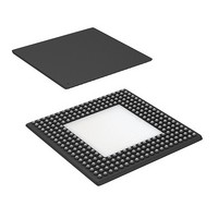
CYV15G0204TRB-BGXC Cypress Semiconductor Corp, CYV15G0204TRB-BGXC Datasheet - Page 8

CYV15G0204TRB-BGXC
Manufacturer Part Number
CYV15G0204TRB-BGXC
Description
IC,TV/VIDEO CIRCUIT,Data Serializer,BICMOS,BGA,256PIN,PLASTIC
Manufacturer
Cypress Semiconductor Corp
Datasheet
1.CYV15G0204TRB-BGXC.pdf
(31 pages)
Specifications of CYV15G0204TRB-BGXC
Function
Serializer/Deserializer
Data Rate
1.485Gbps
Input Type
LVTTL
Output Type
PECL
Number Of Inputs
4
Number Of Outputs
4
Voltage - Supply
3.15 V ~ 3.45 V
Operating Temperature
0°C ~ 70°C
Mounting Type
Surface Mount
Package / Case
256-LBGA Exposed Pad, 32-HLBGA
Lead Free Status / RoHS Status
Lead free / RoHS Compliant
Available stocks
Company
Part Number
Manufacturer
Quantity
Price
Company:
Part Number:
CYV15G0204TRB-BGXC
Manufacturer:
Cypress Semiconductor Corp
Quantity:
135
Company:
Part Number:
CYV15G0204TRB-BGXC
Manufacturer:
Cypress
Quantity:
80
Company:
Part Number:
CYV15G0204TRB-BGXC
Manufacturer:
CYPRESS
Quantity:
216
Company:
Part Number:
CYV15G0204TRB-BGXC
Manufacturer:
Cypress Semiconductor Corp
Quantity:
10 000
Document Number : 38-02101 Rev. *D
Pin Definitions
CYV15G0204TRB HOTLink II Dual Serializer and Dual Reclocking Deserializer
Notes
TXDA[7:0]
TXDB[7:0]
TXERRA
TXERRB
REFCLKA±
REFCLKB±
TXCLKA
TXCLKB
TXCLKOA
TXCLKOB
2. When REFCLKx± is configured for half-rate operation, these inputs are sampled relative to both the rising and falling edges of the associated REFCLKx±.
3. When REFCLKx± is configured for half-rate operation, these outputs are presented relative to both the rising and falling edges of the associated REFCLKx±.
Name
Transmit Path Data and Status Signals
Transmit Path Clock Signals
LVTTL Input,
synchronous,
sampled by the
associated
TXCLKx or
REFCLKx
LVTTL Output,
synchronous to
REFCLKx
asynchronous to
transmit channel
enable / disable,
asynchronous to loss
or return of
REFCLKx±
Differential LVPECL
or single-ended
LVTTL input clock
LVTTL Clock Input,
internal pull-down
LVTTL Output
I/O Characteristics Signal Description
[2]
[3]
,
Transmit Data Inputs. TXDx[9:0] data inputs are captured on the rising edge of the
transmit interface clock. The transmit interface clock is selected by the TXCKSELx
latch via the device configuration interface.
Transmit Path Error. TXERRx is asserted HIGH to indicate detection of a transmit
Phase-Align Buffer underflow or overflow. If an underflow or overflow condition is
detected, TXERRx, for the channel in error, is asserted HIGH and remains asserted
until the transmit Phase-Align Buffer is re-centered with the PABRSTx latch via the
device configuration interface. When TXBISTx = 0, the BIST progress is presented
on the associated TXERRx output. The TXERRx signal pulses HIGH for one
transmit-character clock period to indicate a pass through the BIST sequence once
every 511 character times.
TXERRx is also asserted HIGH, when any of the following conditions is true:
Reference Clock. REFCLKx± clock inputs are used as the timing references for the
transmit PLL. These input clocks may also be selected to clock the transmit parallel
interface. When driven by a single-ended LVCMOS or LVTTL clock source, connect
the clock source to either the true or complement REFCLKx input, and leave the
alternate REFCLKx input open (floating). When driven by an LVPECL clock source,
the clock must be a differential clock, using both inputs.
Transmit Path Input Clock. When configuration latch TXCKSELx = 0, the
associated TXCLKx input is selected as the character-rate input clock for the
TXDx[9:0] input. In this mode, the TXCLKx input must be frequency-coherent to its
associated TXCLKOx output clock, but may be offset in phase by any amount. Once
initialized, TXCLKx is allowed to drift in phase as much as ±180 degrees. If the input
phase of TXCLKx drifts beyond the handling capacity of the Phase Align Buffer,
TXERRx is asserted to indicate the loss of data, and remains asserted until the
Phase Align Buffer is initialized. The phase of the TXCLKx input clock relative to its
associated REFCLKx± is initialized when the configuration latch PABRSTx is written
as 0. When the associated TXERRx is deasserted, the Phase Align Buffer is
initialized and input characters are correctly captured.
Transmit Clock Output. TXCLKOx output clock is synthesized by each channel’s
transmit PLL and operates synchronous to the internal transmit character clock.
TXCLKOx operates at either the same frequency as REFCLKx± (TXRATEx = 0), or
at twice the frequency of REFCLKx± (TXRATEx = 1). The transmit clock outputs
have no fixed phase relationship to REFCLKx±.
• The TXPLL for the associated channel is powered down. This occurs when OE2x
• The absence of the REFCLKx± signal.
and OE1x for a given channel are both disabled by setting OE2x = 0 and OE1x = 0.
CYV15G0204TRB
Page 8 of 31
[+] Feedback


